-
ProblemsWafer Scratching
Wafer Sticking
Misalignment
Contact Damage -
Proposed EffectWafer Scratch Prevention
Misalignment Prevention
Contact Damage Reduction
Yield Improvement -
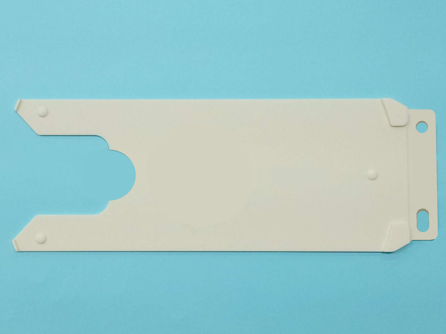
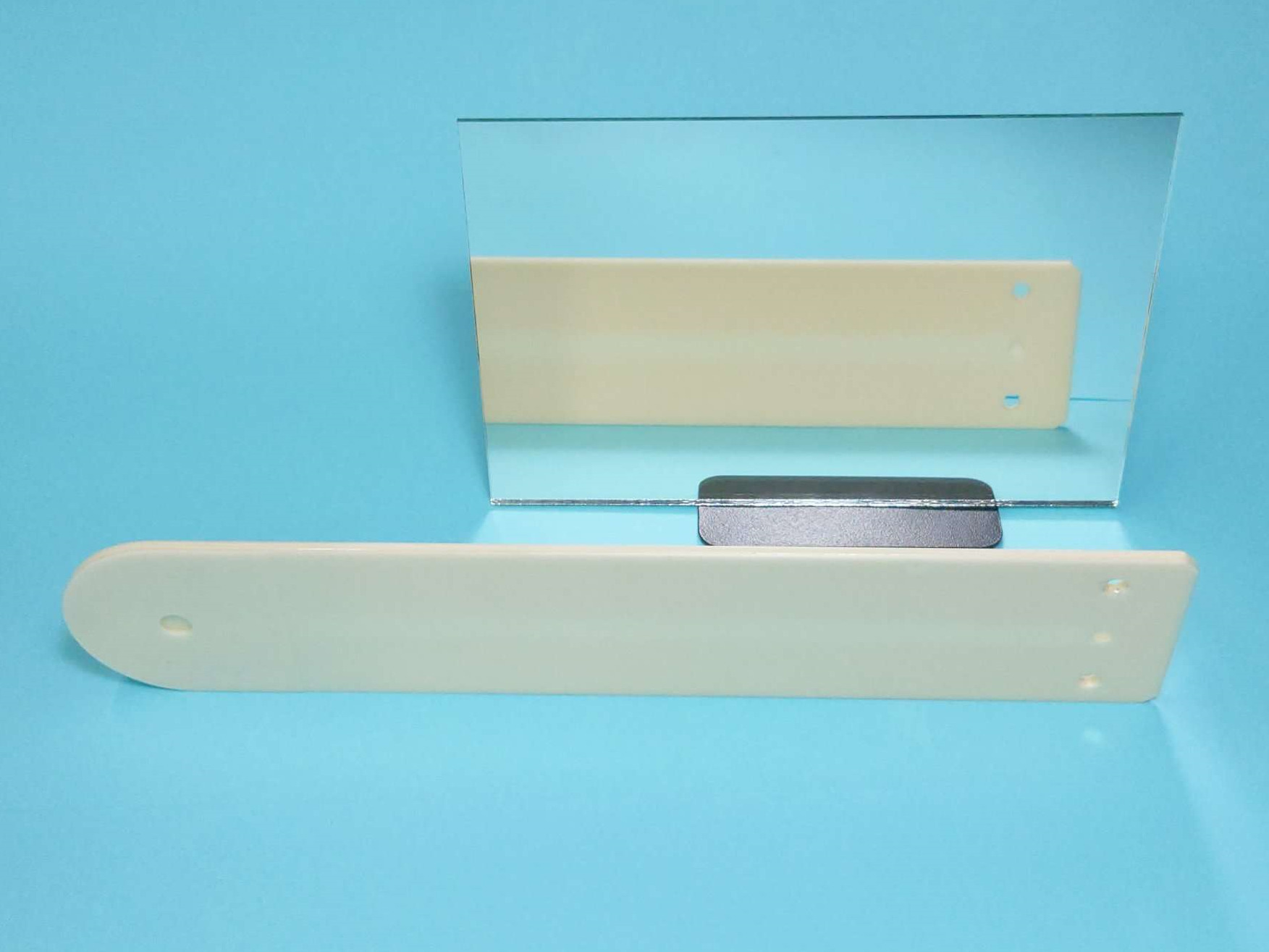
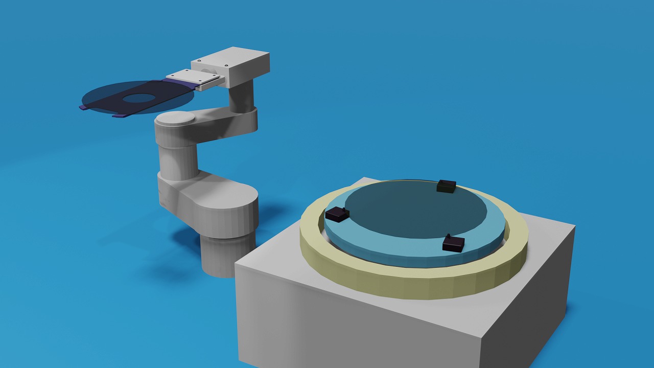
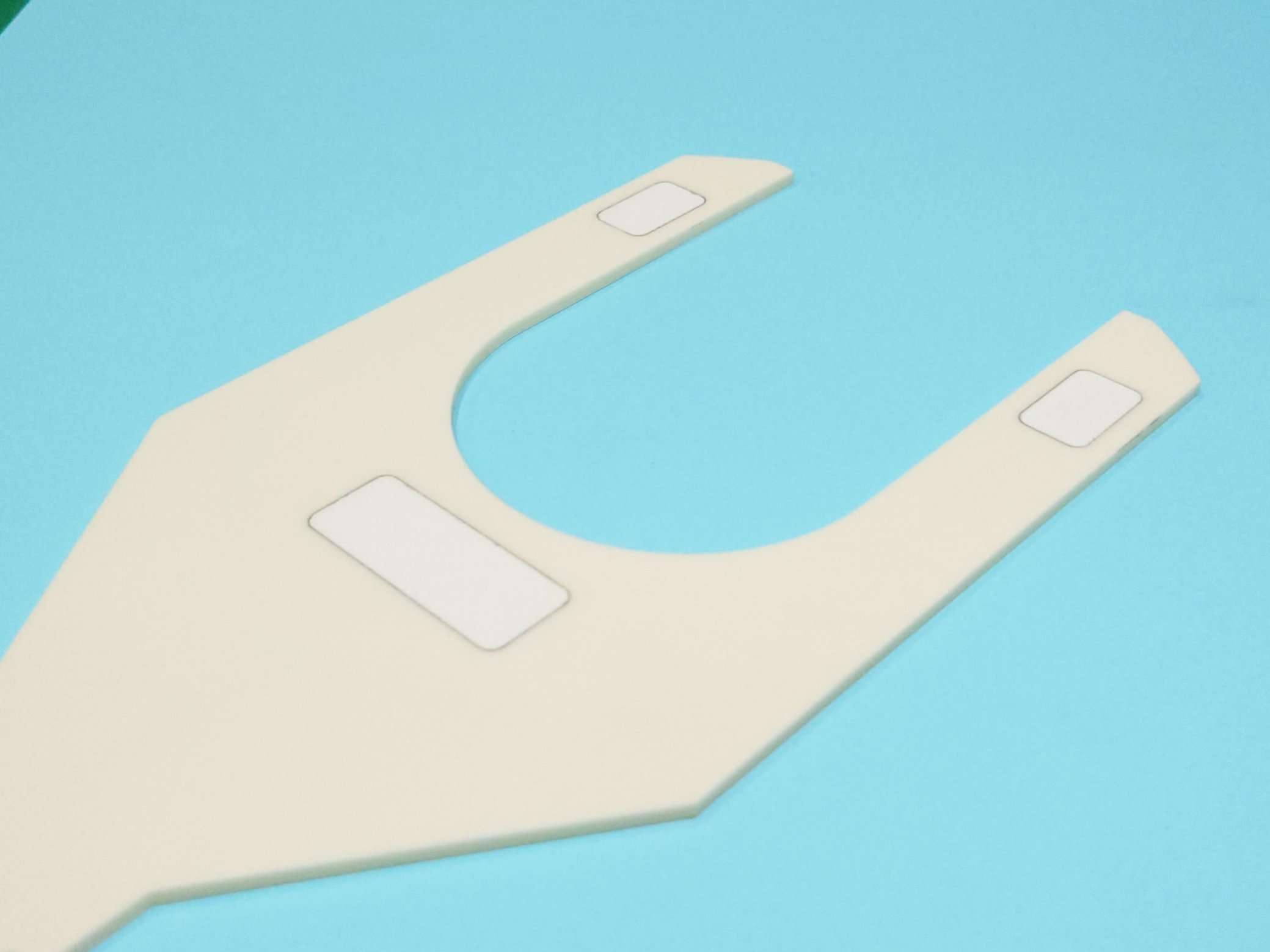
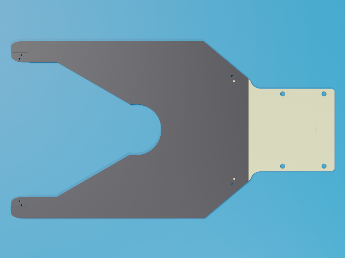
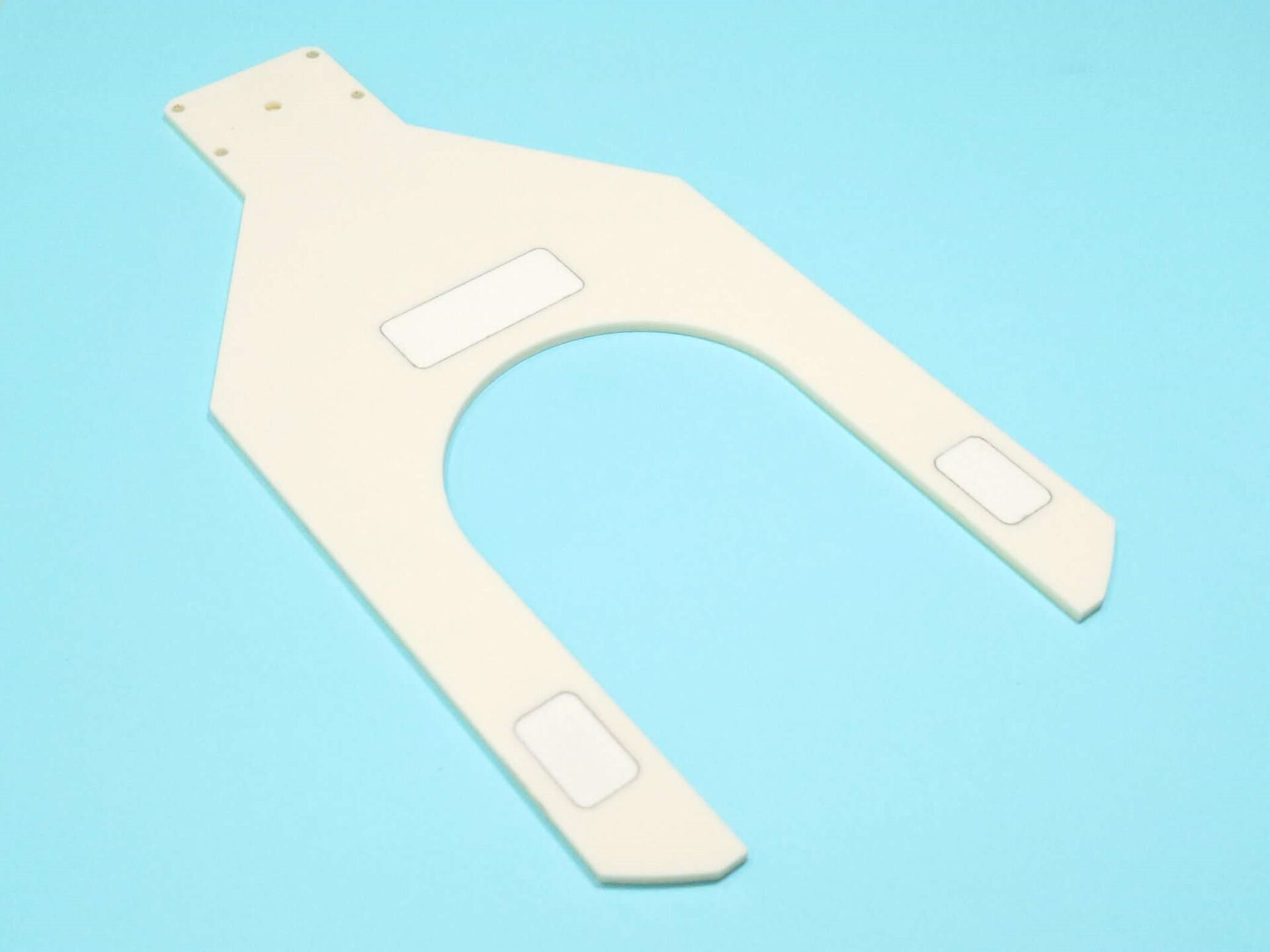
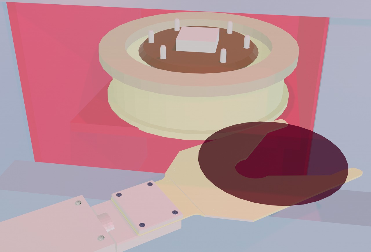
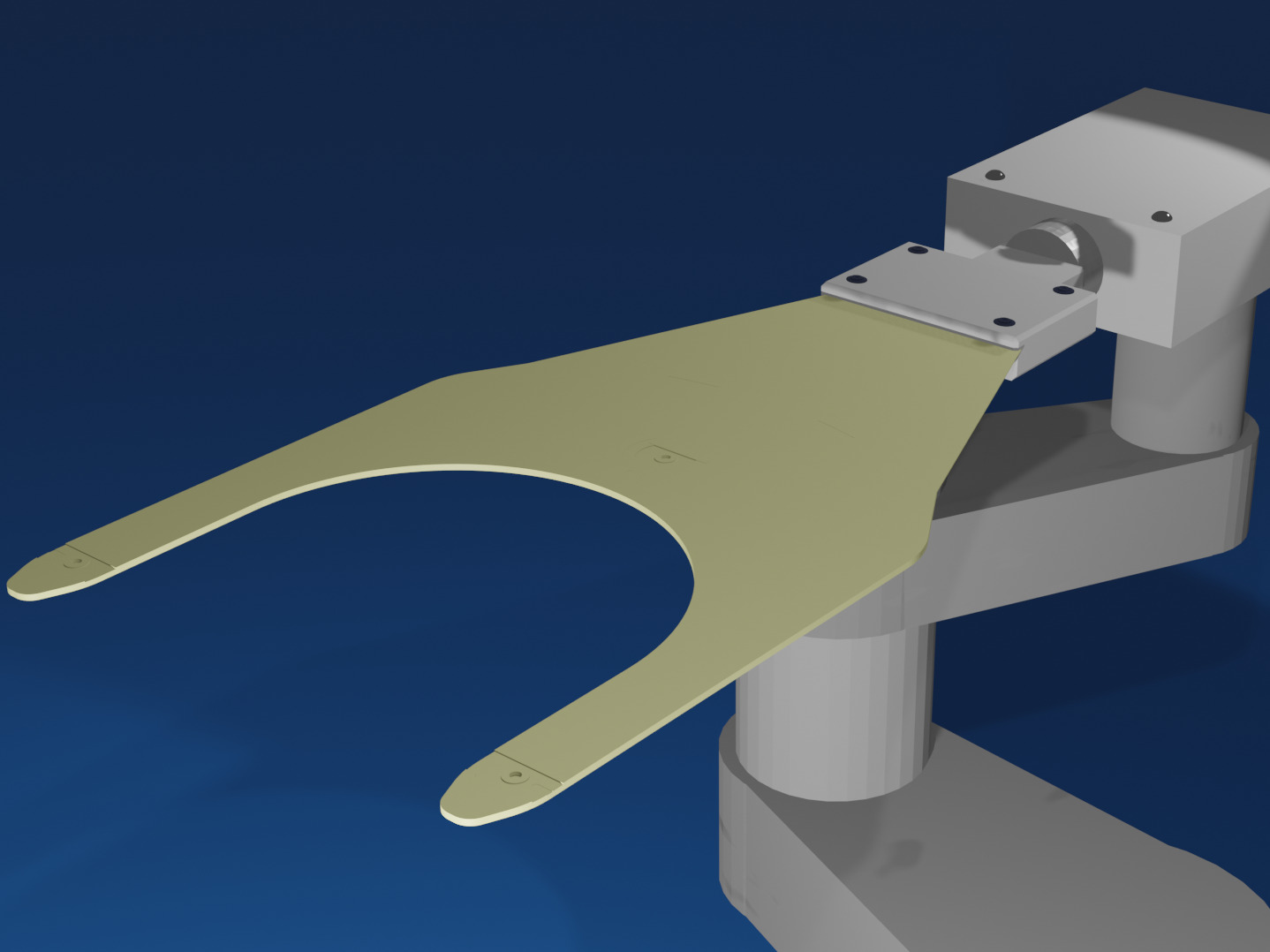
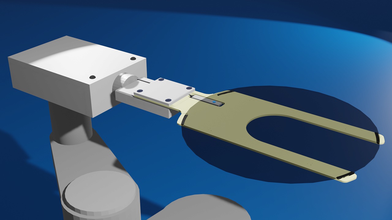
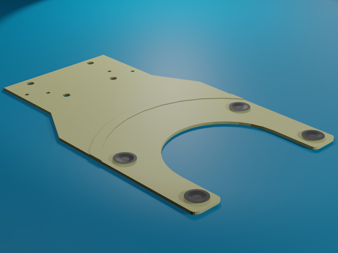
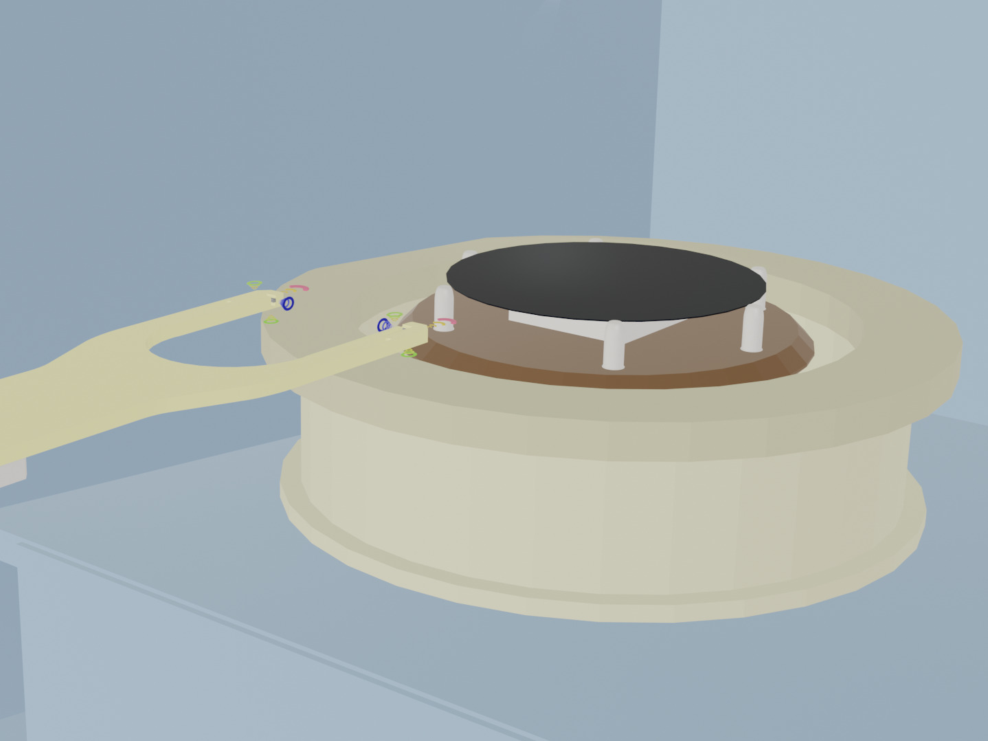
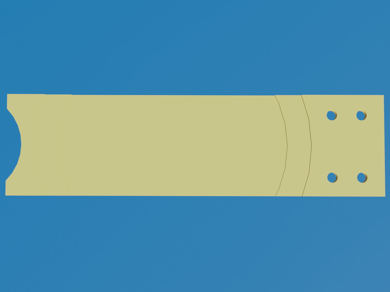
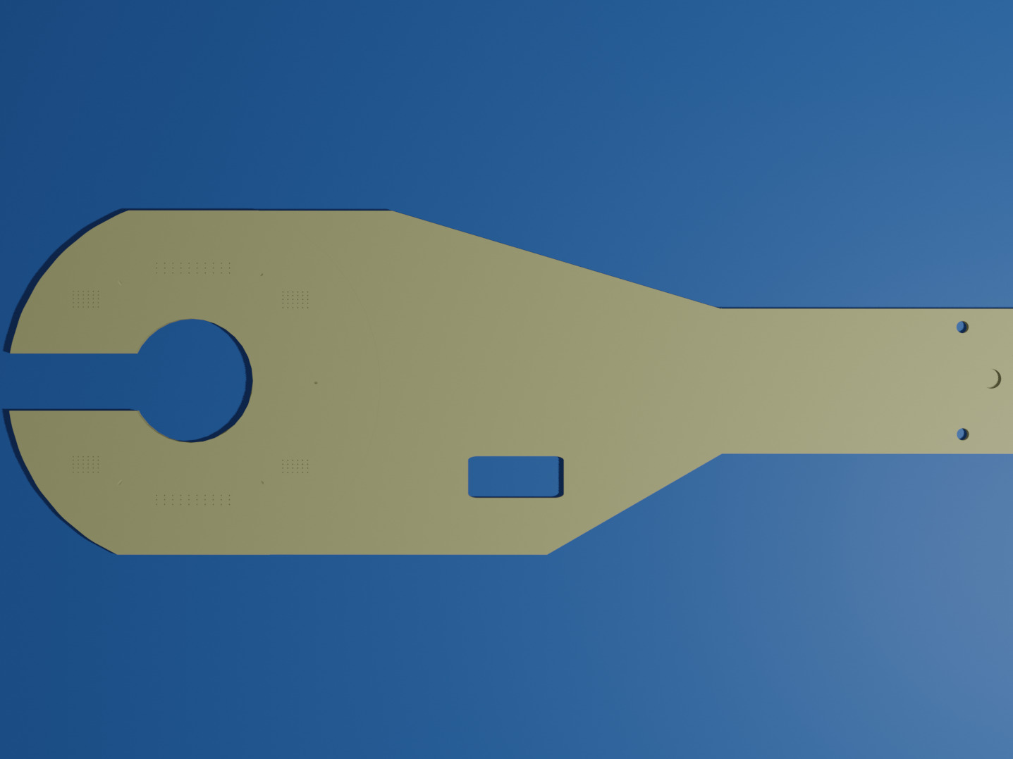
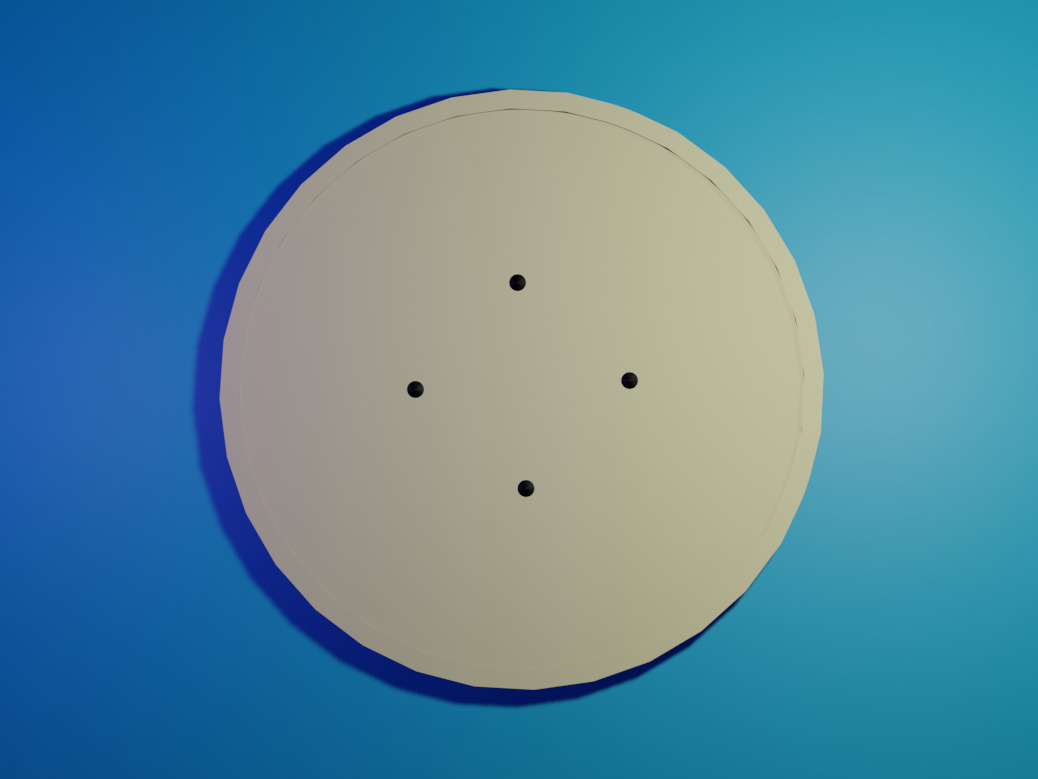
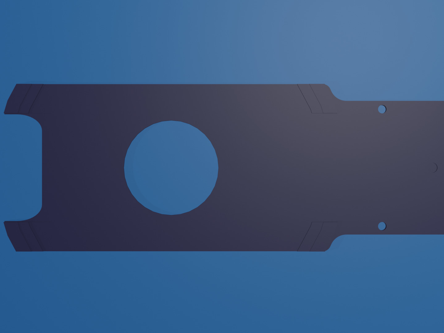
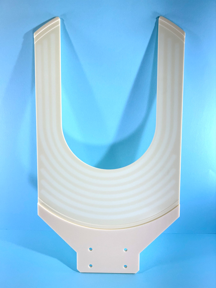
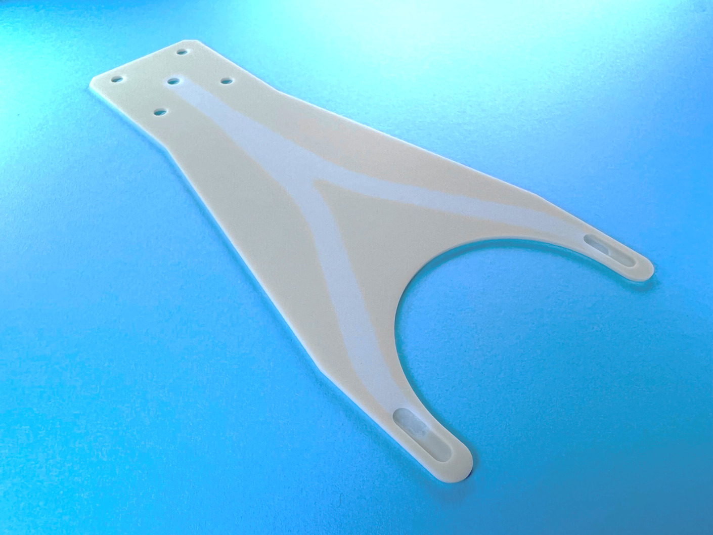
Product TypeWafer Transfer End Effector / Handling ArmPAD
Customer's concerns and problems / Before
Our proposals and improvement effects / After
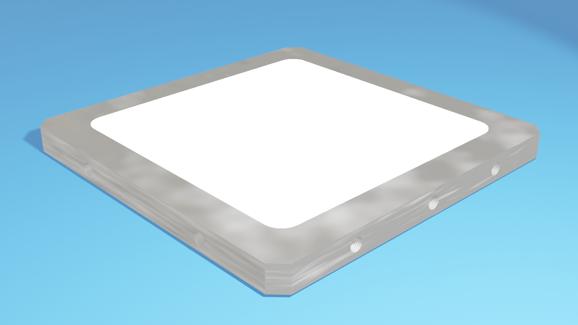
The surface-treatment developed by ASUZAC for PAD was implemented to make it difficult for PAD to stick to the wafer.
This helped to prevent misalignment and scratches.


Point of the proposed example / Point
The point of this case is that the productivity was improved by changing the coating without changing the shape of the parts.
Asuzac focuses on material development and coating development, and it is possible to add new characteristics to parts without changing the base material or part shape.
Especially, this approach is effective for preventing static electricity and contamination.
The Fine Ceramics Division of ASUZAC Corporation, which operates the Ceramics Design Laboratory, handles everything from material development and preparation to design and manufacture, as well as surface treatment, inspection, and cleaning.
We can also offer our own coating-technology for adding functionality to ceramics materials, as well as the selection of materials such as ceramic materials with high heat resistance and conductivity, and high-purity alumina and SiC that are highly pure and prevent contamination.
If you have any trouble with the existing PAD, please do not hesitate to contact us.
Integrated response from processing to development of ceramic materials !
Please feel free to contact us !
Business hours: 9:00-17:00 (closed on Saturdays, Sundays and Holidays)


.jpg)


.jpg)


The use of fluoroplastic PAD has caused the wafer to stick to PAD.
In particular, when the surface roughness of PAD is rough, the wafers tend to stick to PAD, and when the wafers are released, they are misaligned and scratched.