-
ProblemsParticles
Suction Marks
Wafer Scratching -
Proposed EffectWafer Scratch Prevention
Warped Wafer Prevention
Suction Mark Reduction
Yield Improvement
Particle Control -
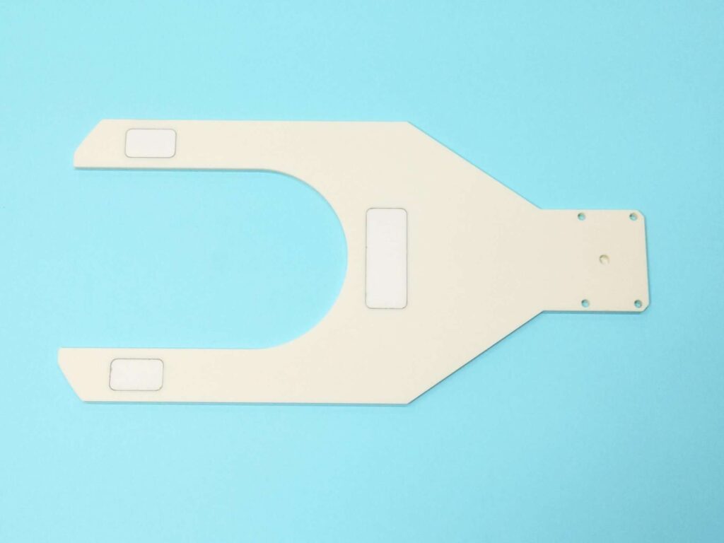
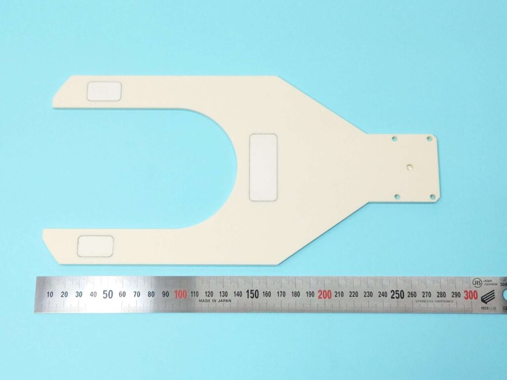
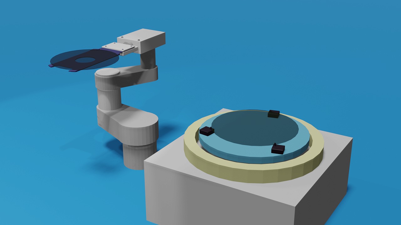
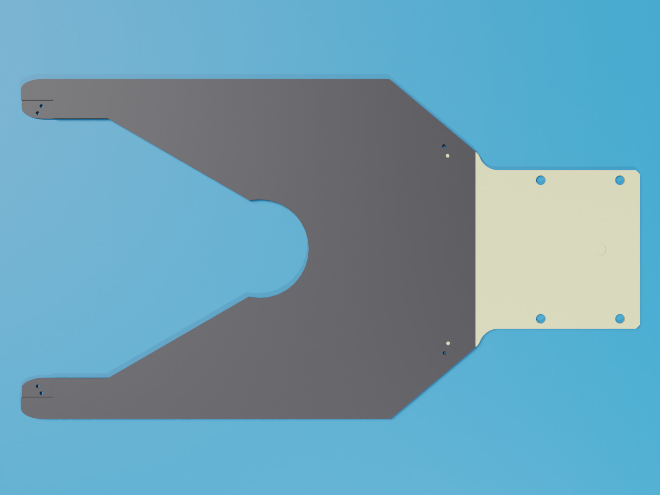
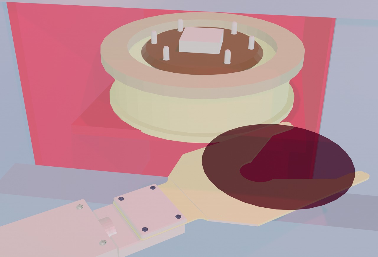
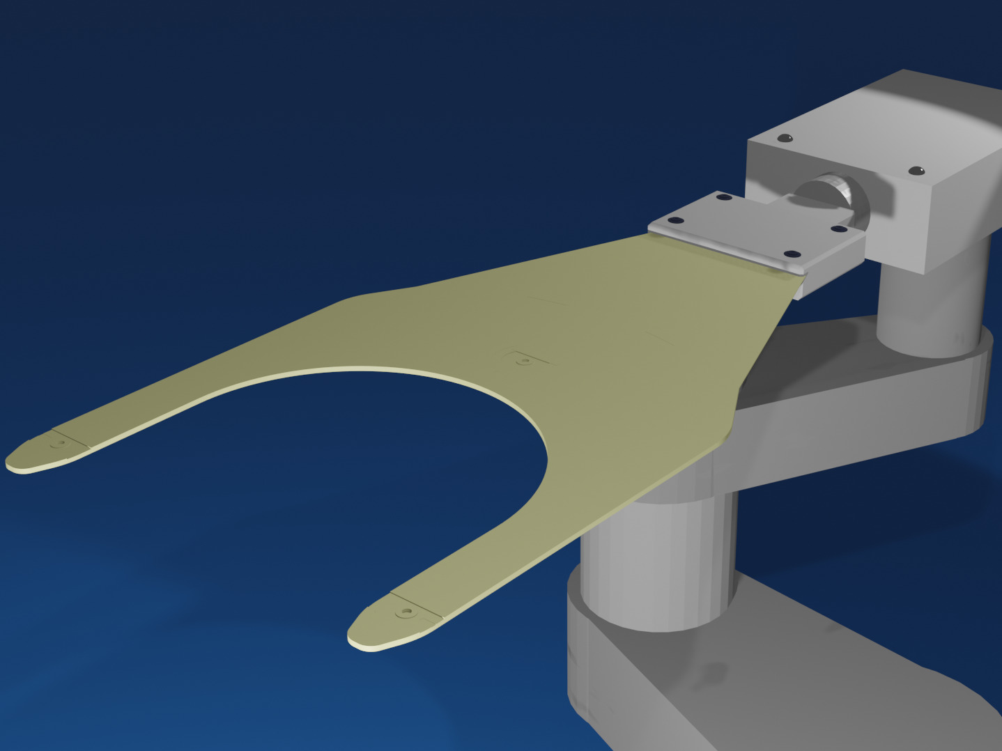
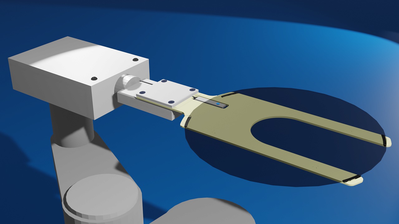
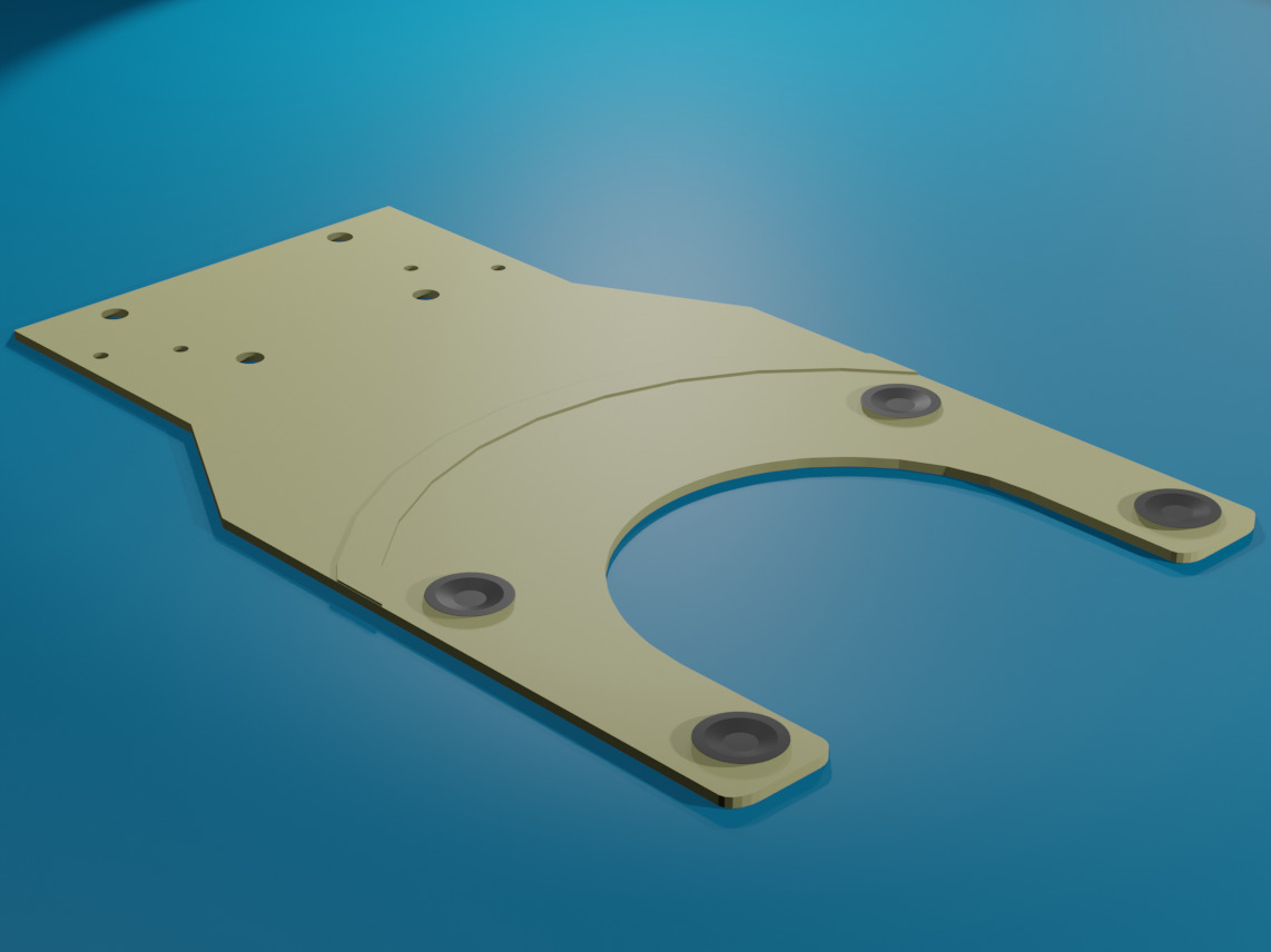
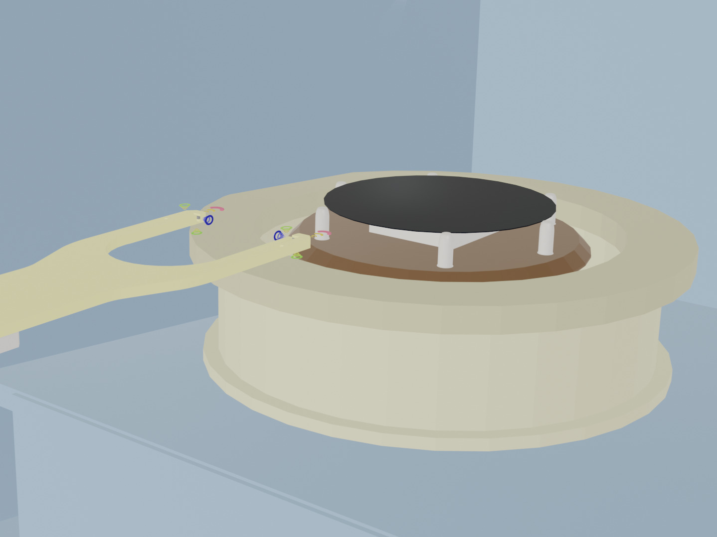
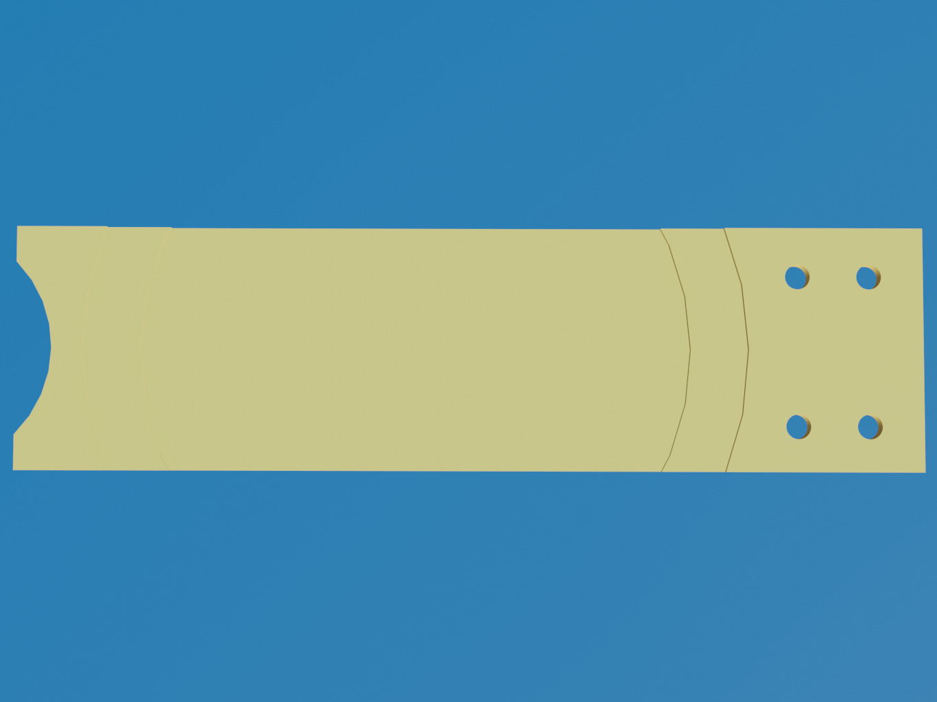
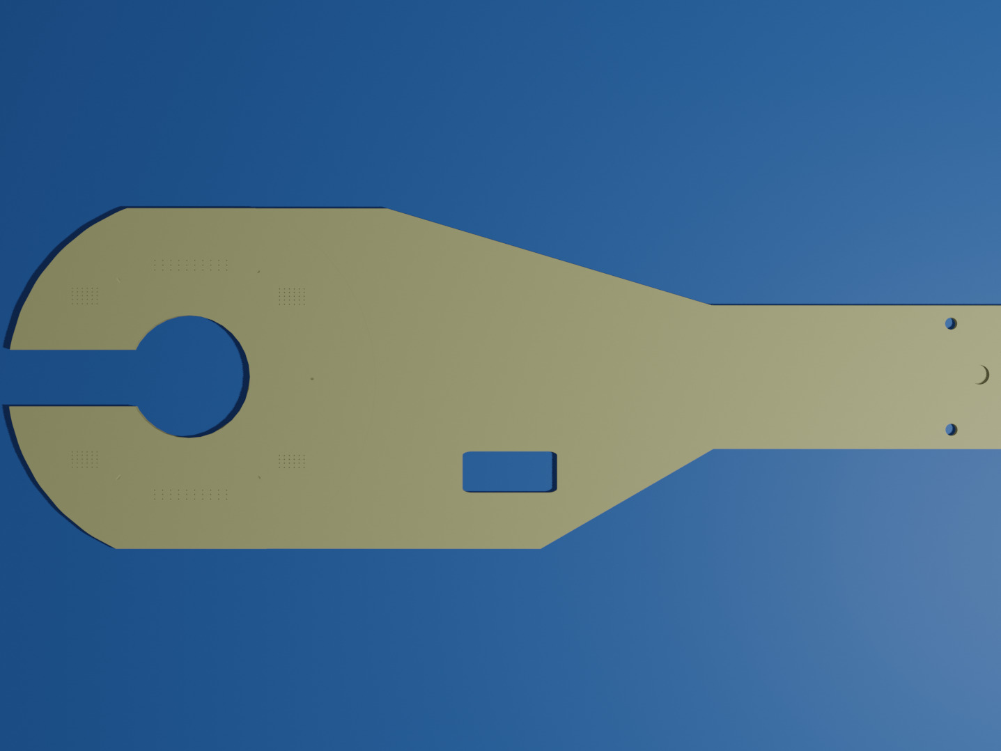
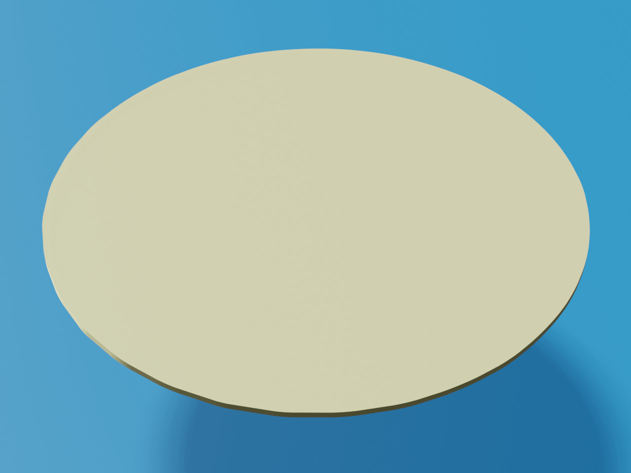
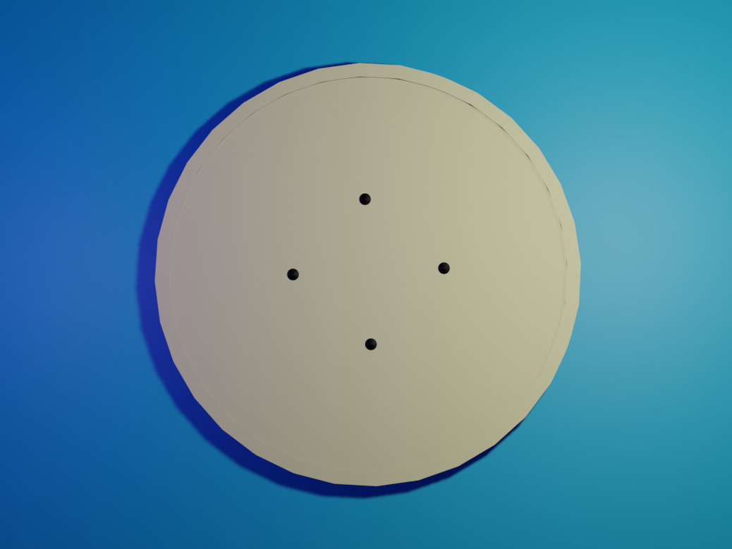
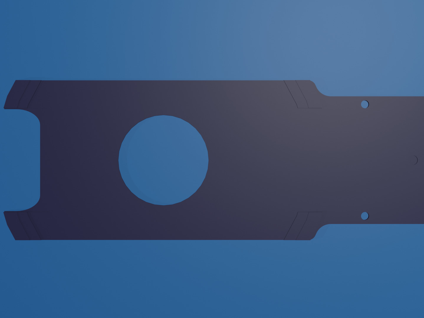
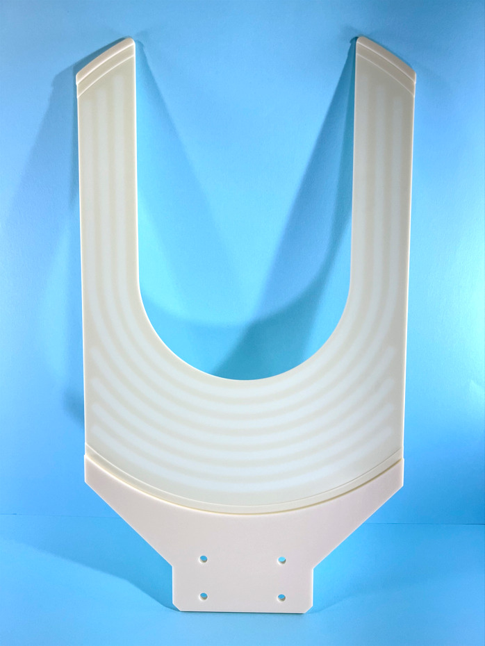
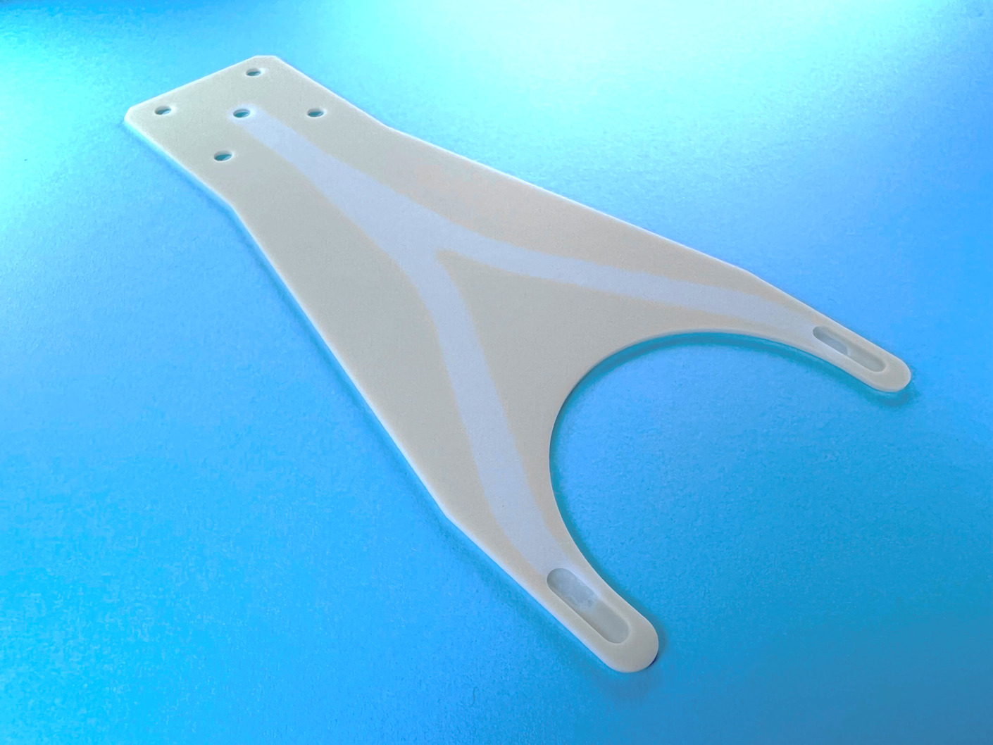
Product TypeWafer Transfer End Effector / Handling Arm
Customer's concerns and problems / Before
Our proposals and improvement effects / After
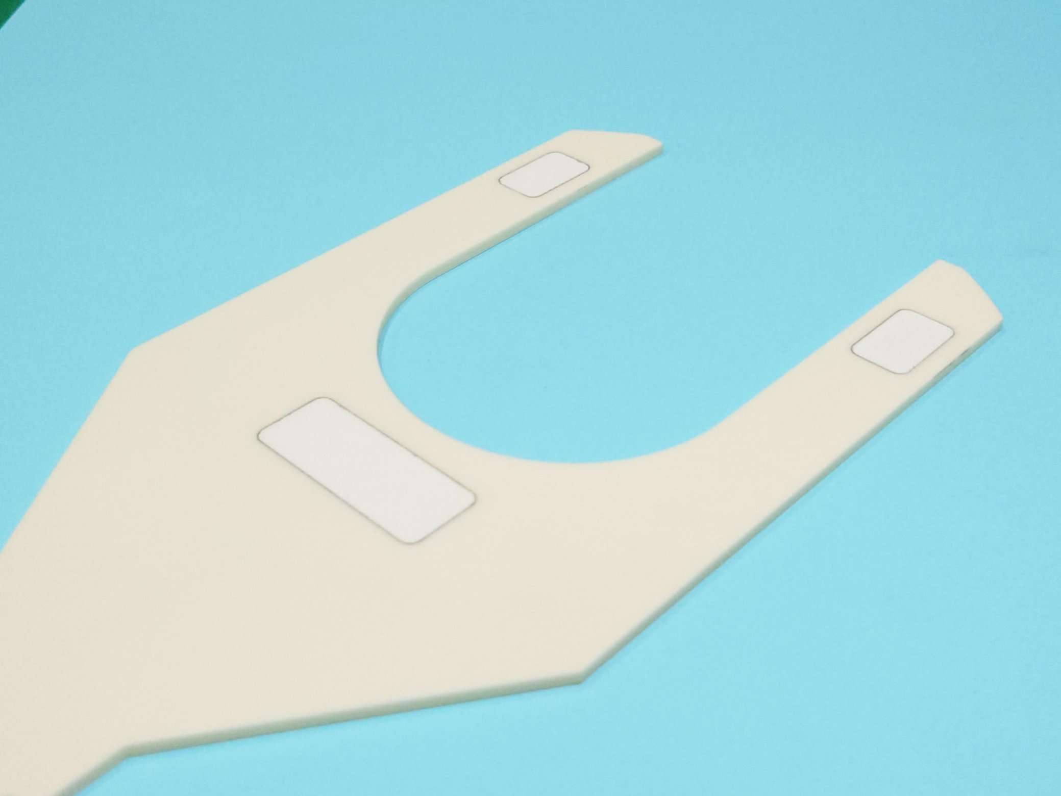
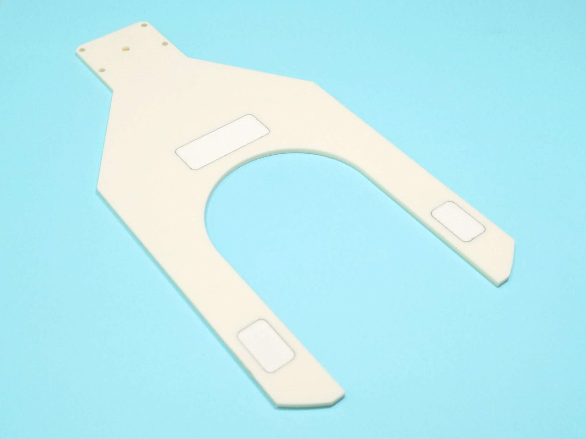
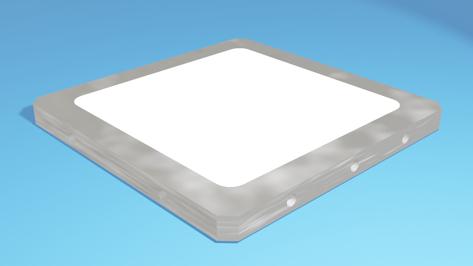
In the past, suction-type Transfer End Effector / Handling Arm were used, but we proposed a porous embedded End Effector / Handling Arm with a coating treatment to prevent suction marks from sticking to the wafer.
Asuzac’s porous ceramics have a hole diameter of 30 to 40μm, which makes it difficult for the wafer to receive suction marks or scratches.
As a result of the customer’s use, it became difficult for the wafer to be attached with suction marks, contributing to the improvement of yield.


Point of the proposed example / Point
The point of this case is that we were able to improve productivity by changing the type of Transfer End Effector / Handling Arm, especially in important processes.
Changing the conveyance method entails risks, but it is possible to greatly achieve the results of new technological developments like porous ceramics, which evolve day by day.
In this case, the use of porous ceramics with fine pore diameters prevents scratches.
The Fine Ceramics Division of ASUZAC Corporation, which operates the Ceramics Design Laboratory, handles everything from material development and preparation to design and manufacture, as well as surface treatment, inspection, and cleaning.
We can also offer our own coating-technology for adding functionality to ceramics materials, as well as the selection of materials such as ceramics materials with high heat resistance and conductivity, and high-purity alumina and SiC that are highly pure and prevent contamination.
If you have trouble with the existing wafer Transfer End Effector / Handling Arm, please feel free to contact us.
Integrated response from processing to development of ceramic materials !
Please feel free to contact us !
Business hours: 9:00-17:00 (closed on Saturdays, Sundays and Holidays)


.jpg)


.jpg)


Our customer had been searching for a solution because of the problem of sticking marks on the wafer.
If there is an adsorption mark on the wafer, particles will be generated, and the yield will be lowered.