-
ProblemsProductivity (Throughput)
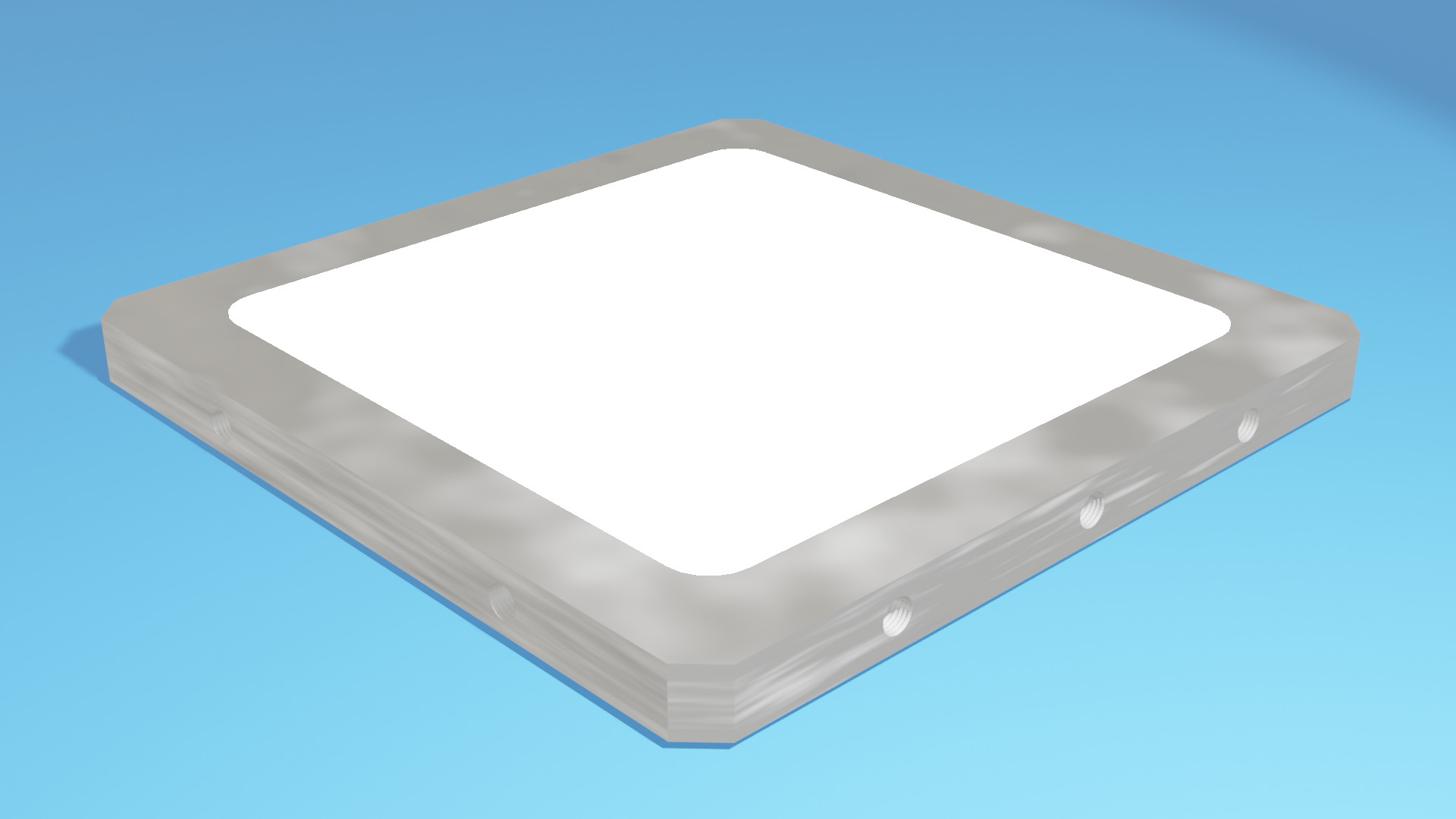
Part Replacement Time -
Proposed EffectImproved Productivity(Improved Throughput)
Improved Functionality -
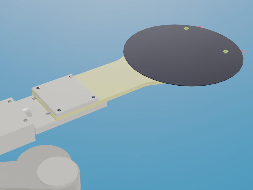
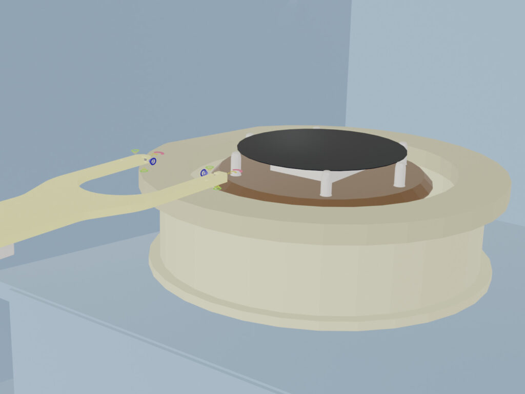
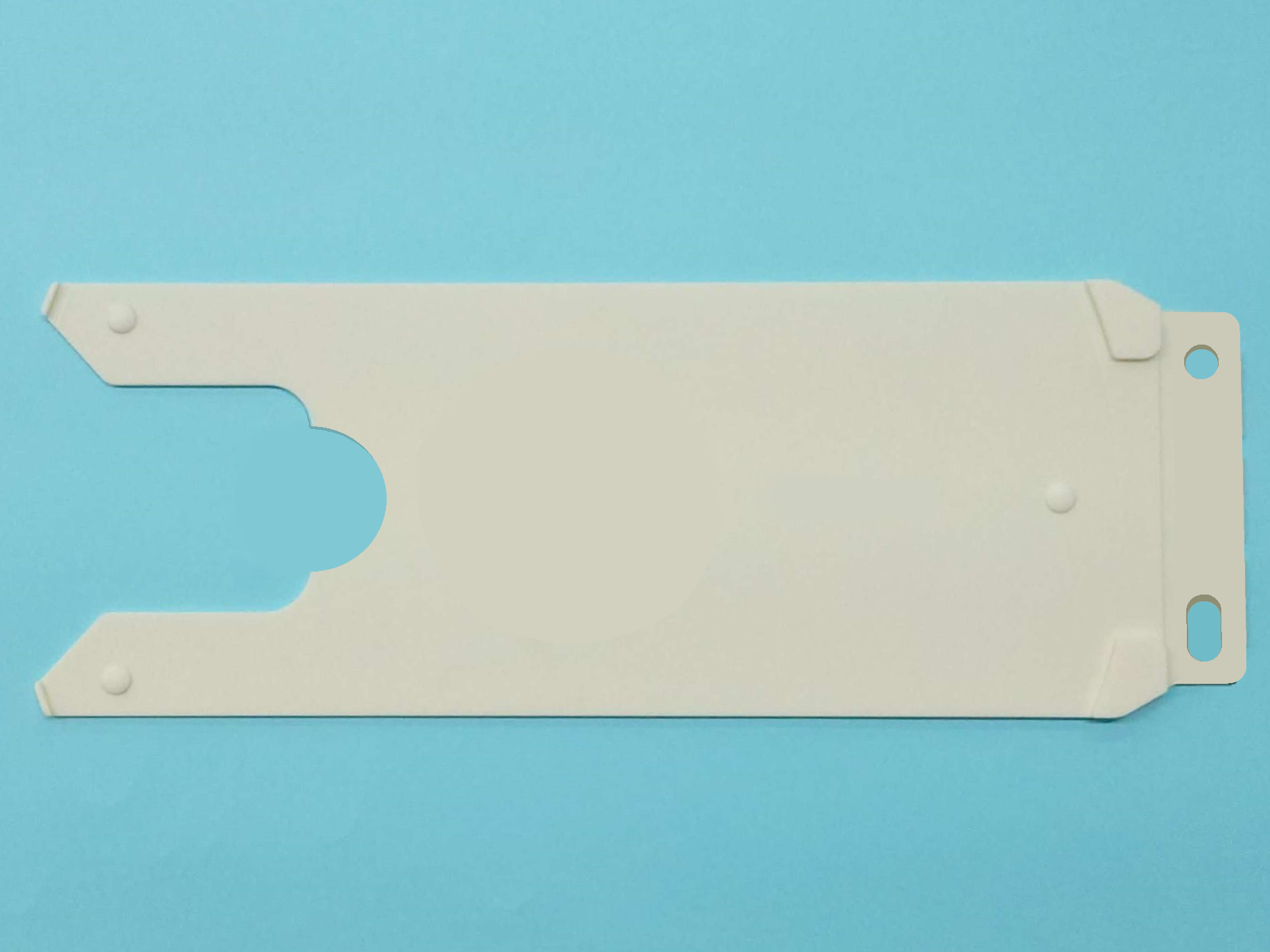
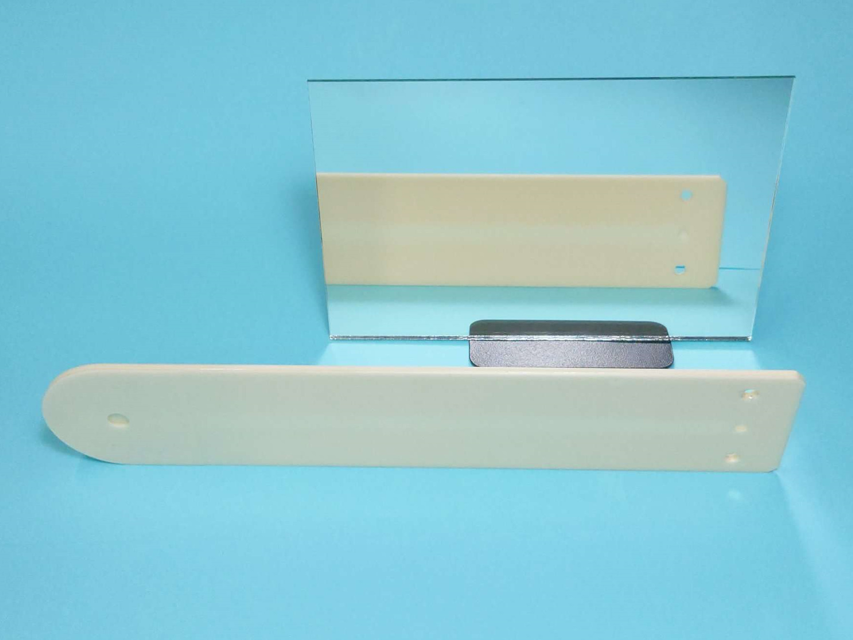
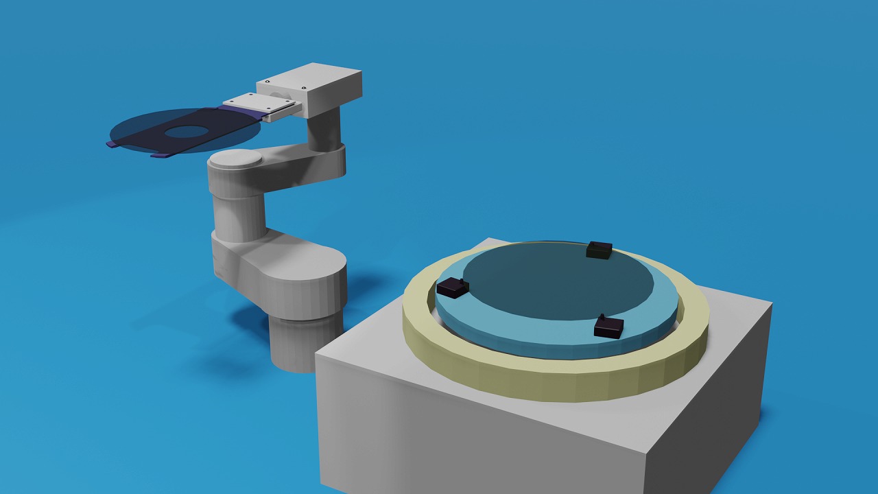
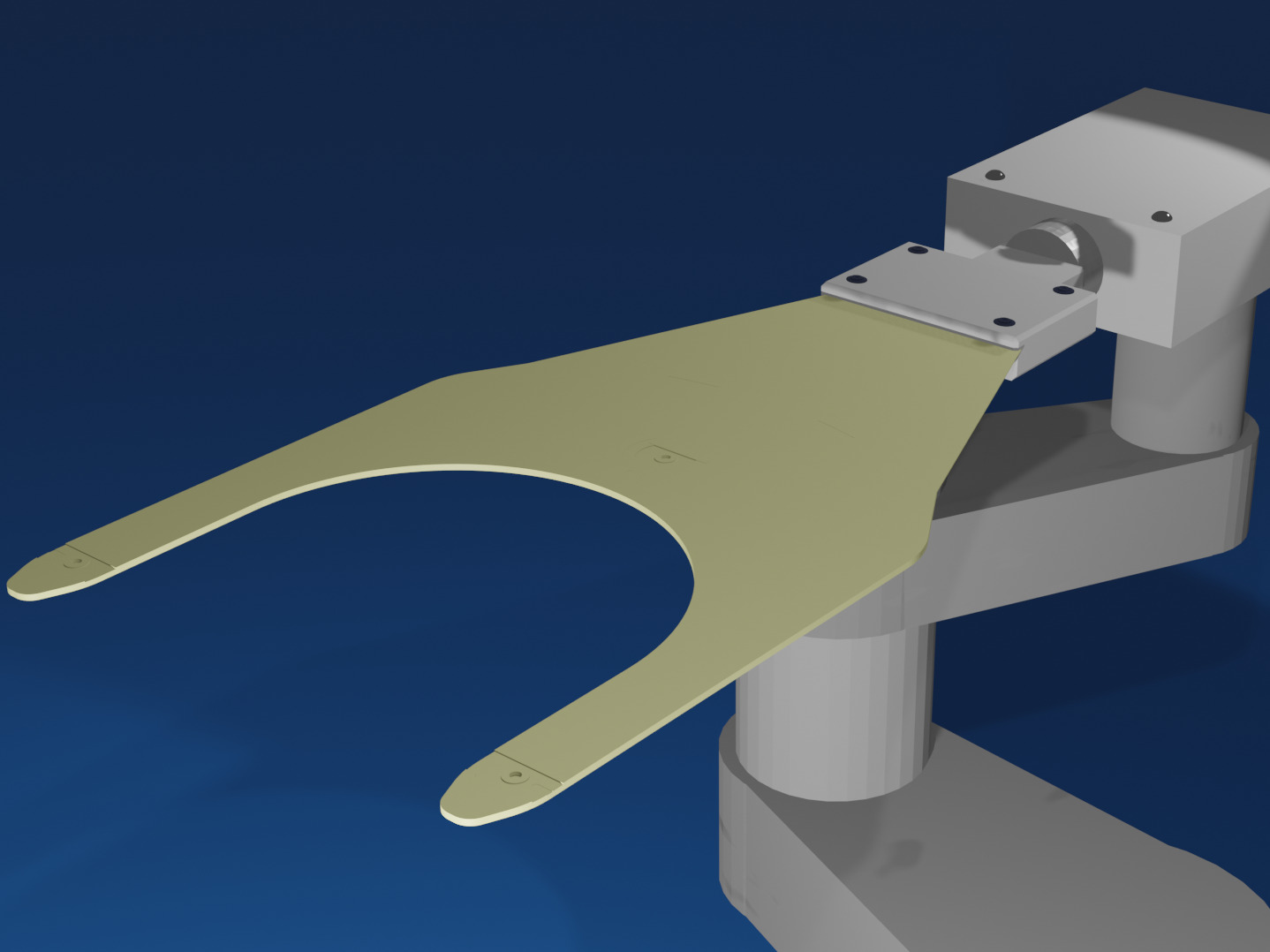
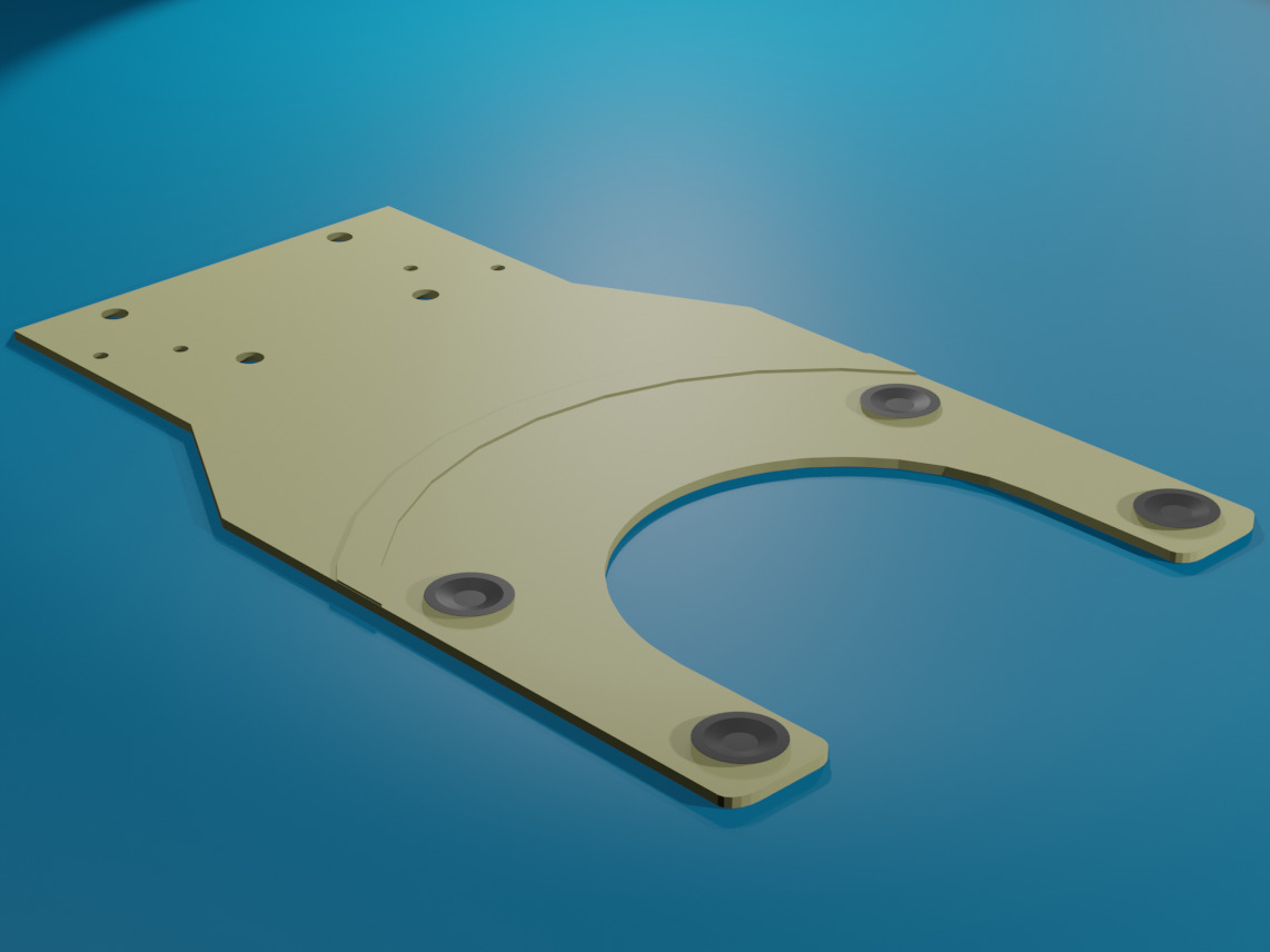
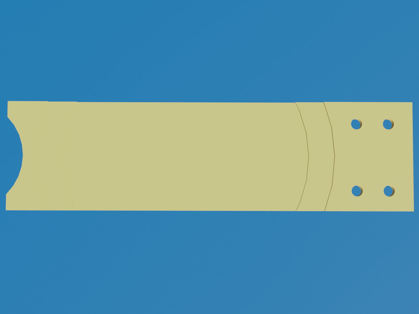
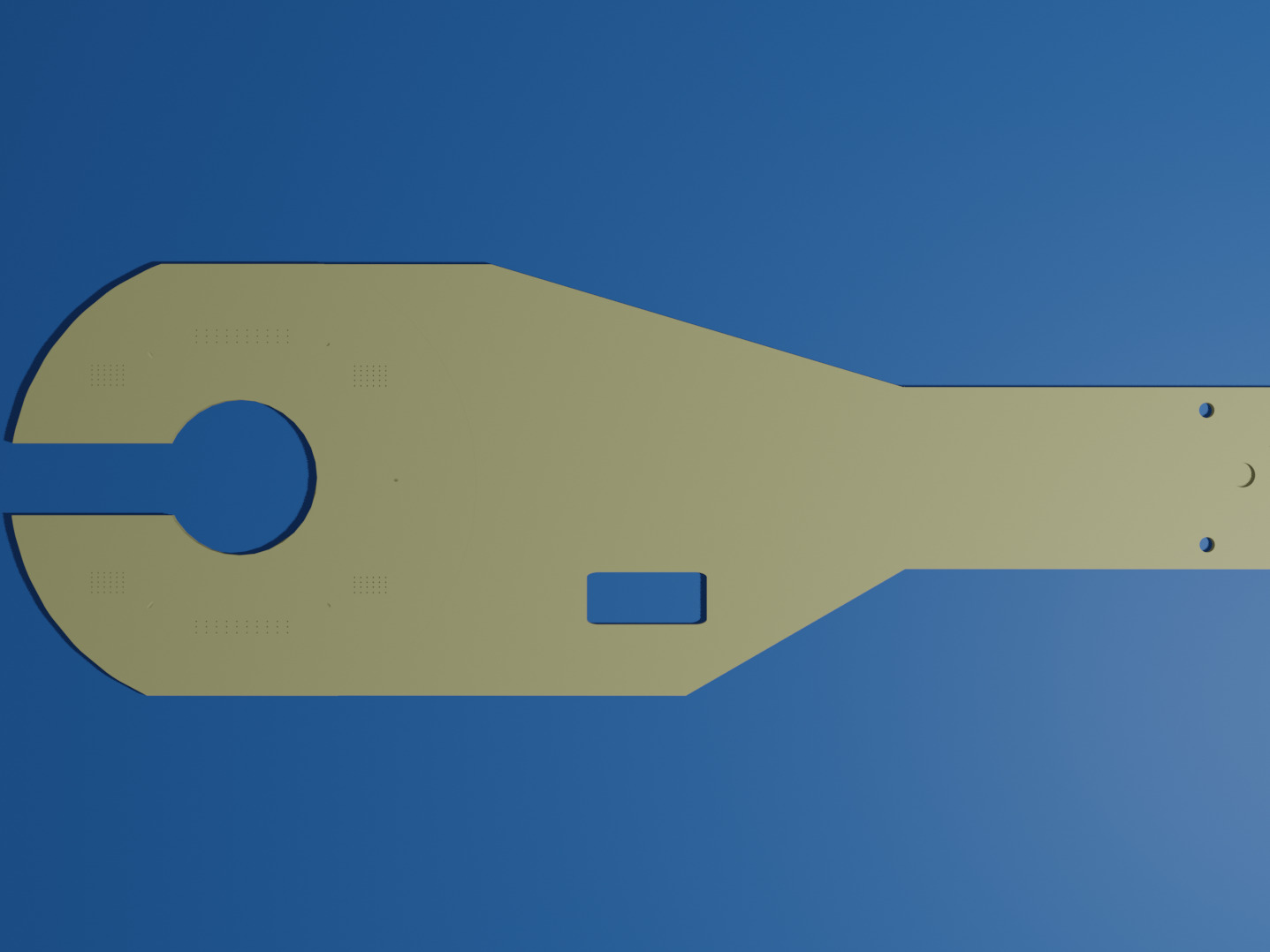
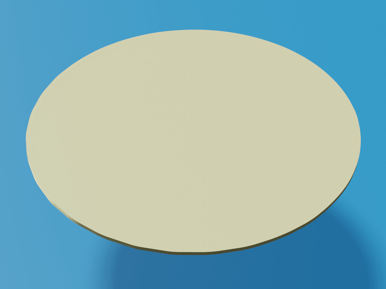
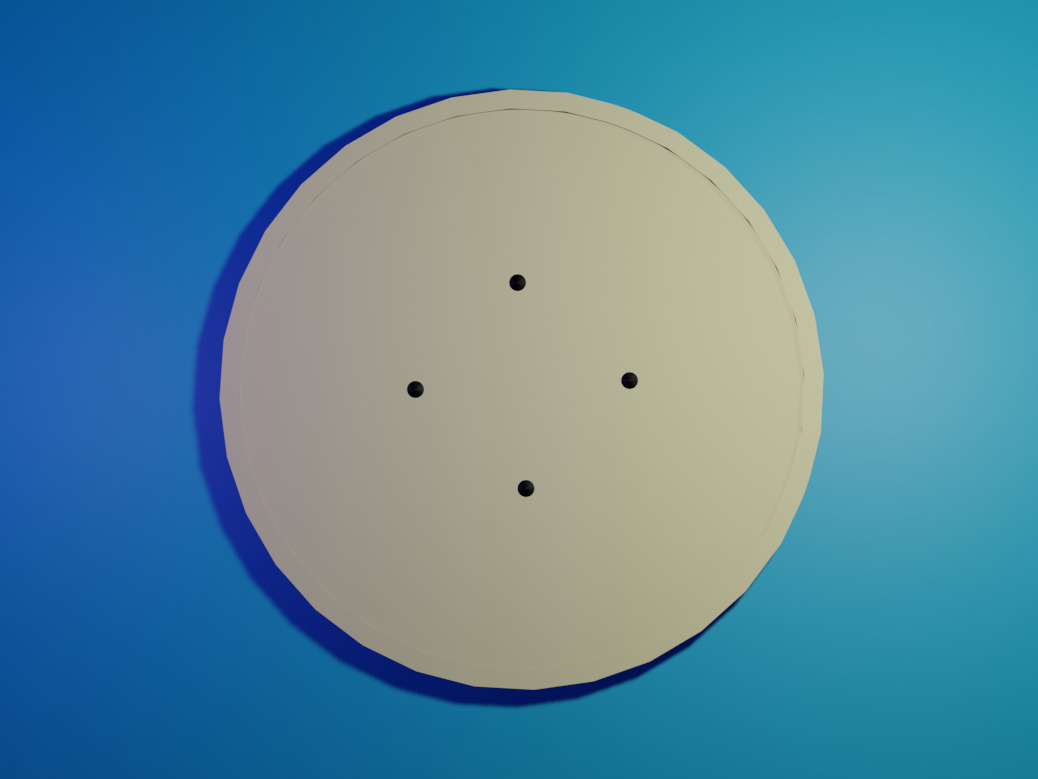
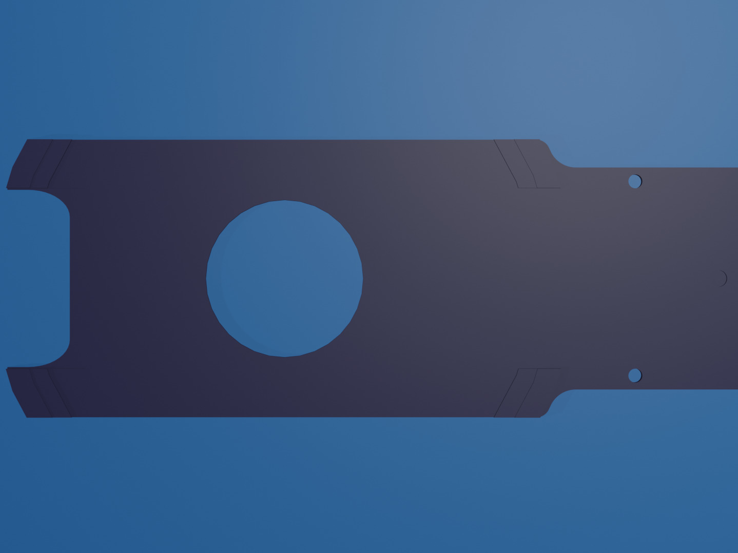
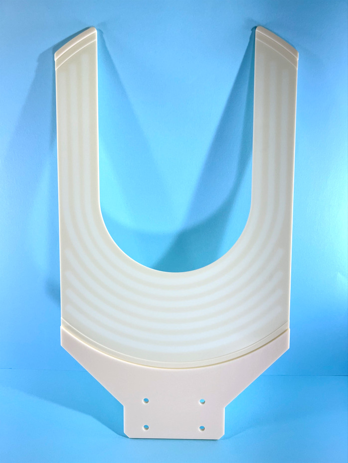
Product TypeWafer Transfer End Effector / Handling Arm
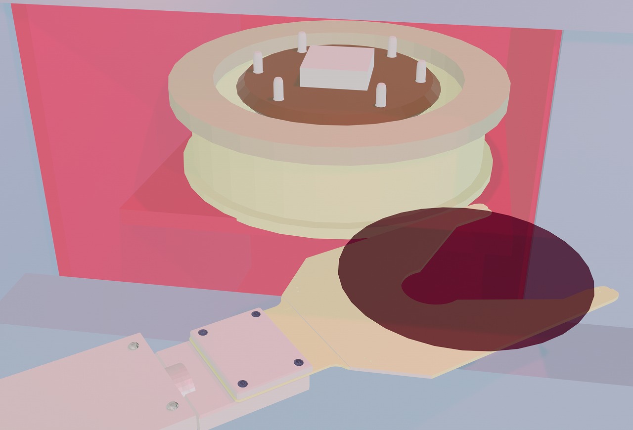
Customer's concerns and problems / Before
Our proposals and improvement effects / After
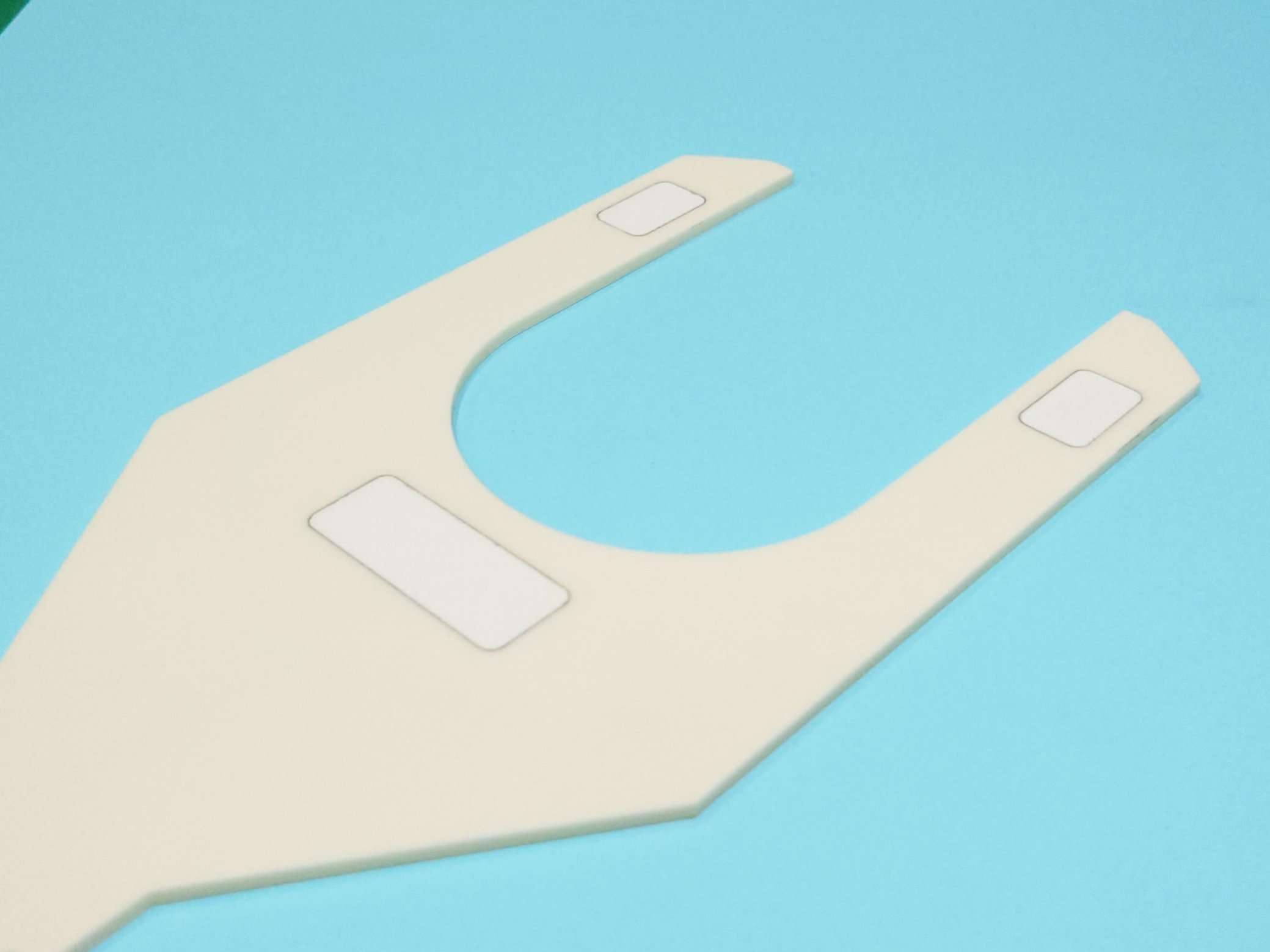
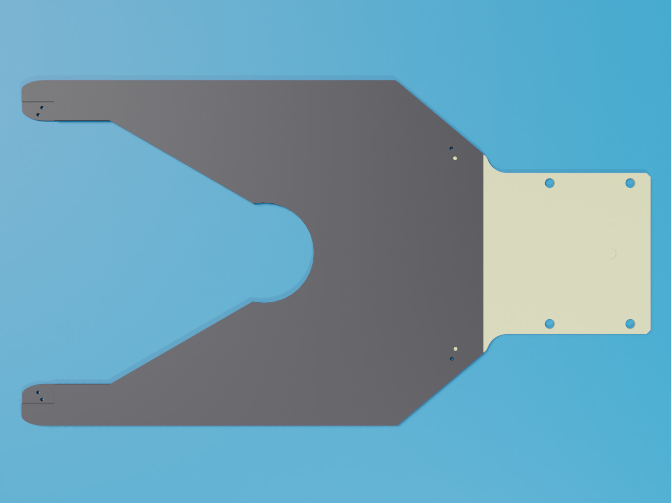
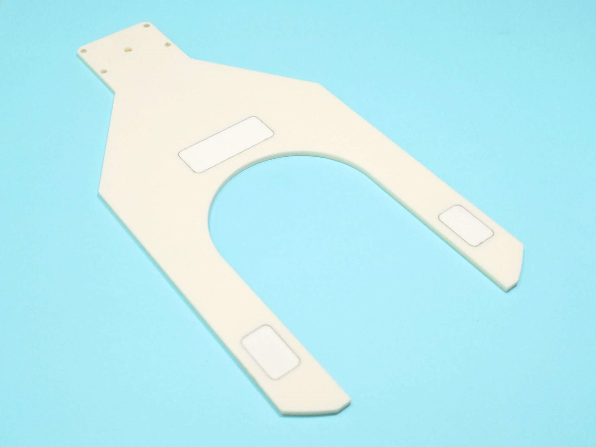
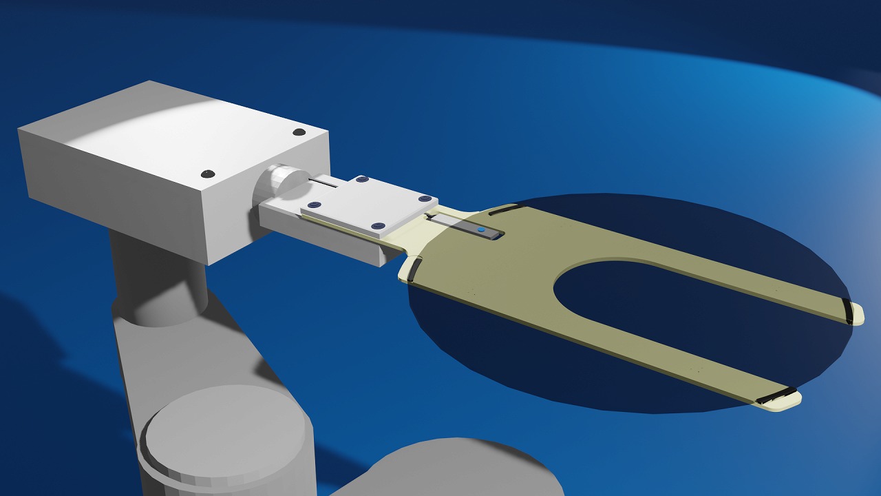
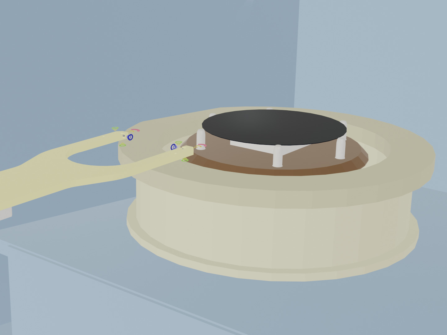
In response, the Ceramics Design Laboratory proposed assembling sensors at the tip of the wafer Transfer End Effector / Handling Arm.
As a result, workers were able to check the consumable rate without opening the chamber, thus realizing improved productivity (improved throughput).
Point of the proposed example / Point
The point of this case is that the assembly of the sensor to the wafer Transfer End Effector / Handling Arm reduces the man-hours required for the replacement and maintenance of the edge ring.
The Fine Ceramics Division of ASUZAC Corporation, which operates the Ceramics Design Laboratory, handles everything from the development and preparation of materials for ceramics to design and manufacture, as well as surface treatment, inspection, and cleaning.
We can also offer our own coating-technology for adding functionality to ceramics materials, as well as the selection of materials such as ceramics materials with high heat resistance and conductivity, and high-purity alumina and SiC that are highly pure and prevent contamination.
We also offer suggestions for reducing man-hours and improving productivity in semiconductor manufacturing processes, so please feel free to contact us.
Integrated response from processing to development of ceramic materials !
Please feel free to contact us !
Business hours: 9:00-17:00 (closed on Saturdays, Sundays and Holidays)


.jpg)


.jpg)
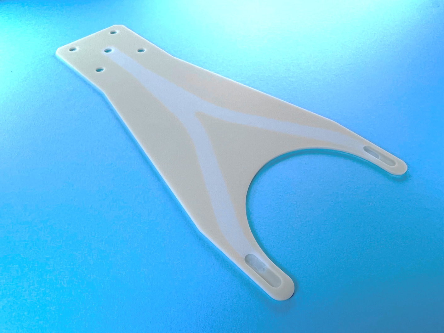


A production engineer from a semiconductor equipment manufacturer asked us, “In the etching process, it is time-consuming to open the chamber every time to check the wear rate of the edge ring. We are looking for a good suggestion.”