-
ProblemsSuction Marks
Wafer Scratching
Wafer Sticking
Air-Permeability -
Proposed EffectWafer Scratch Prevention
Suction Mark Reduction -
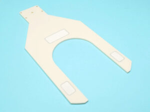
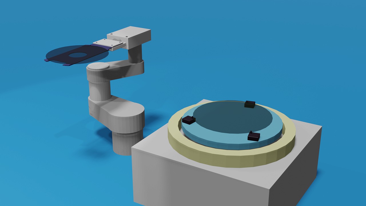
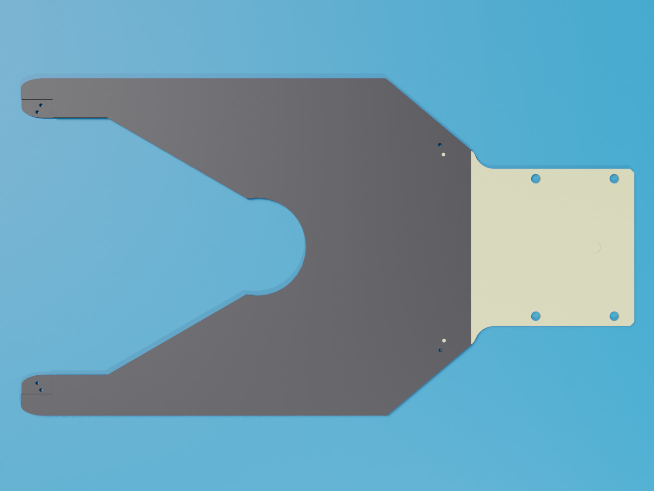
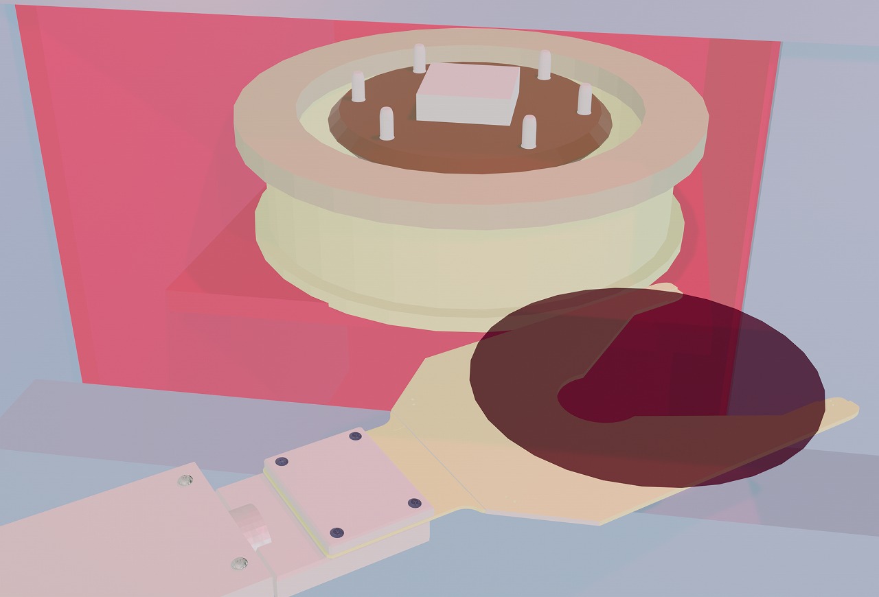
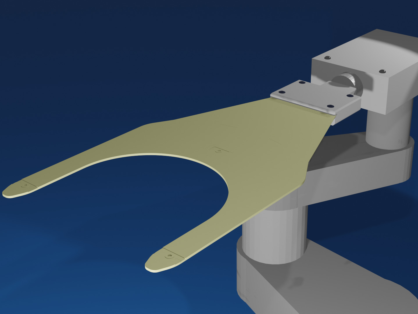
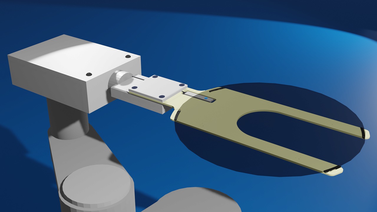
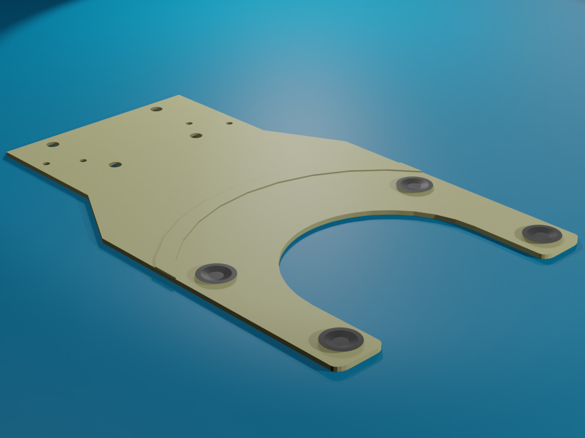
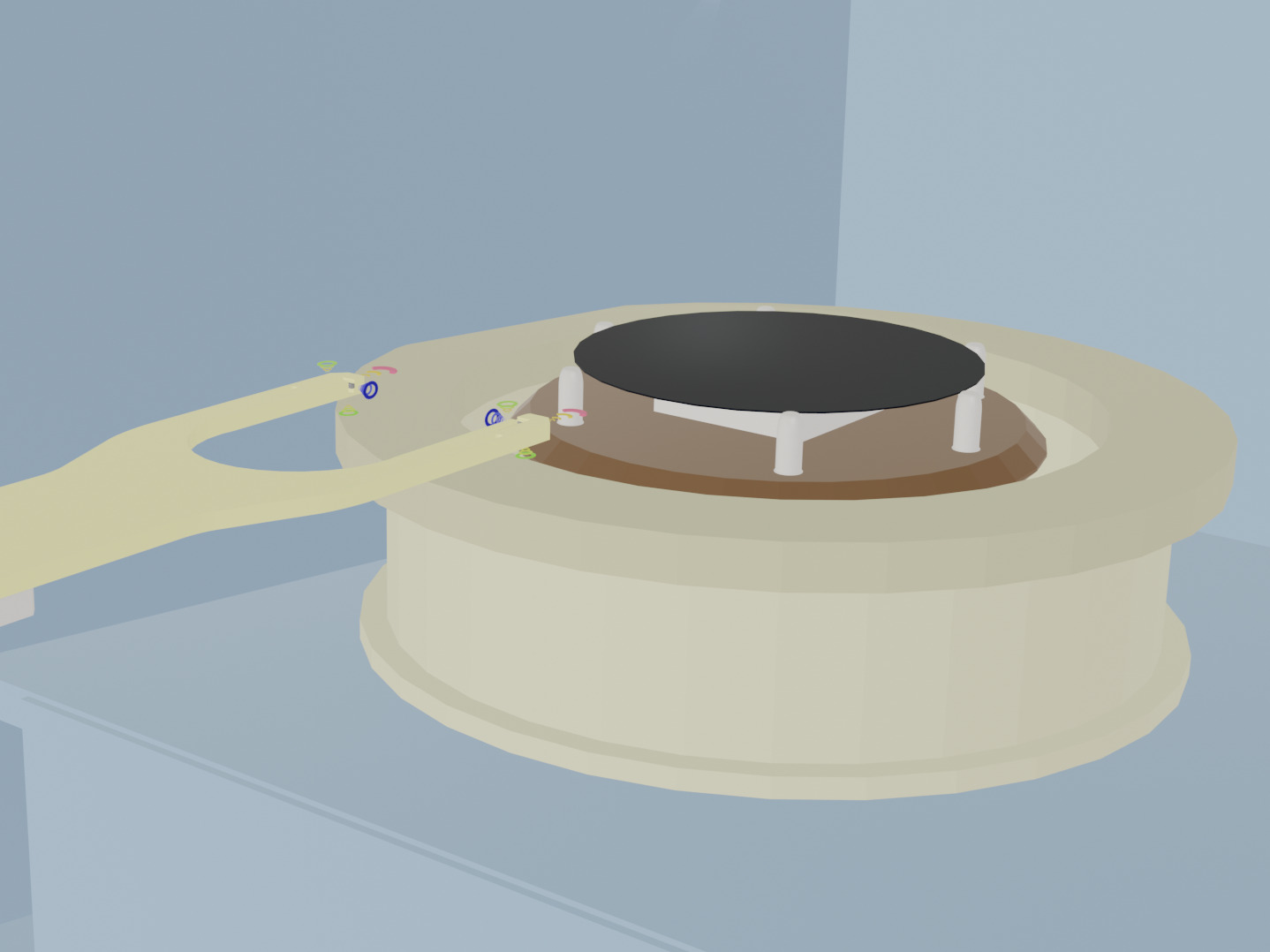
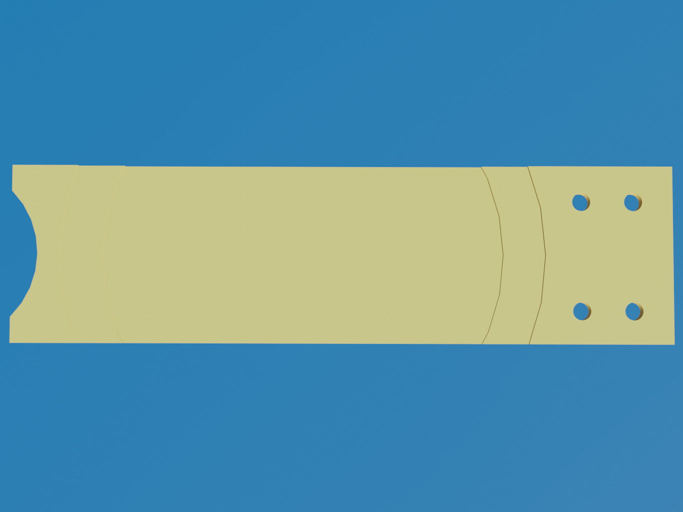
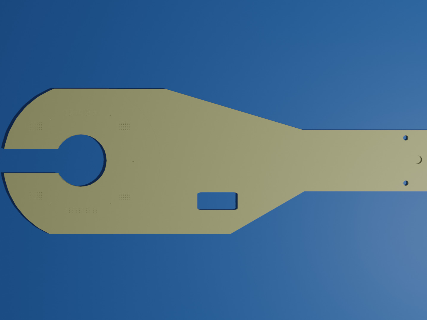
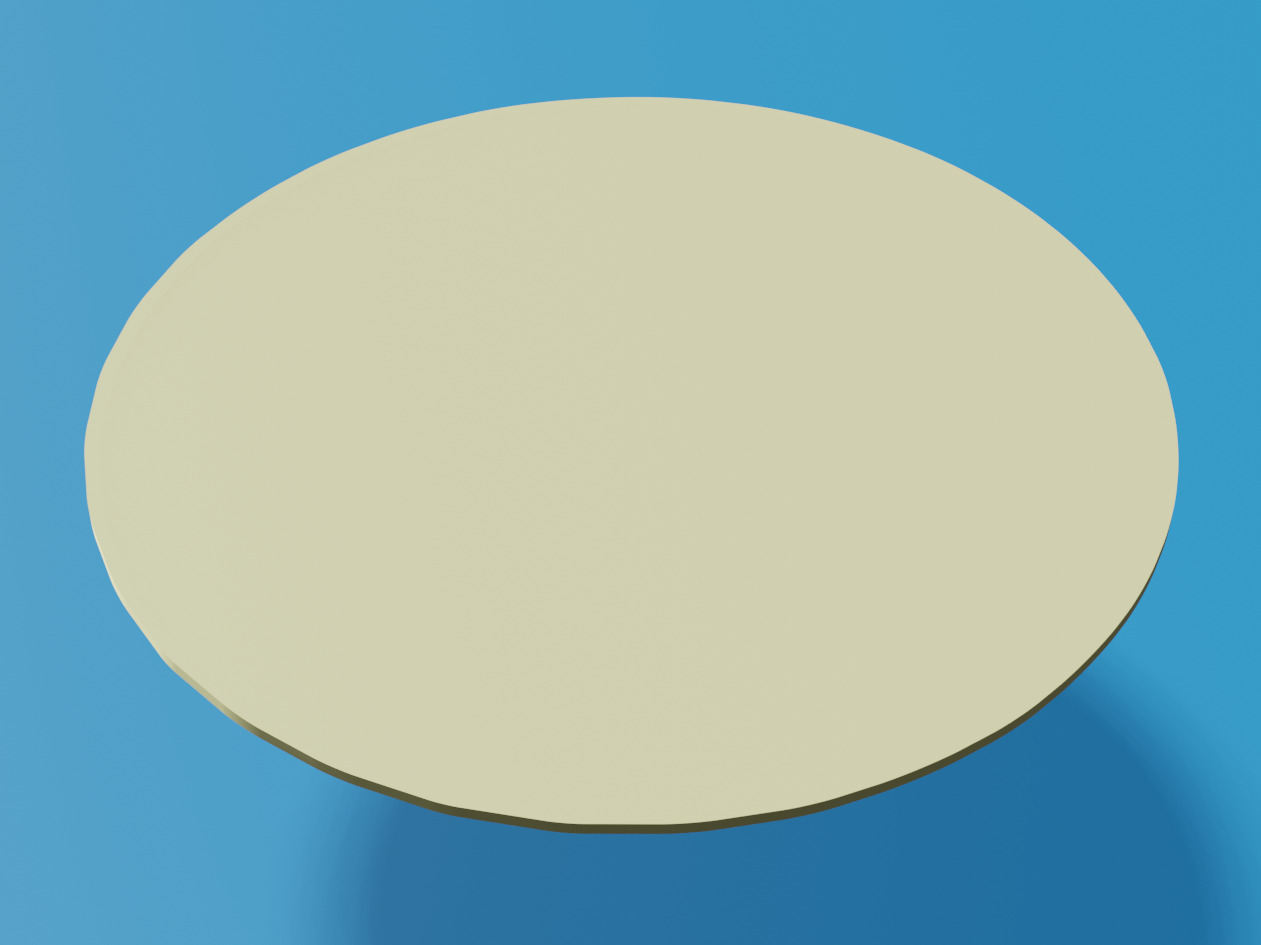
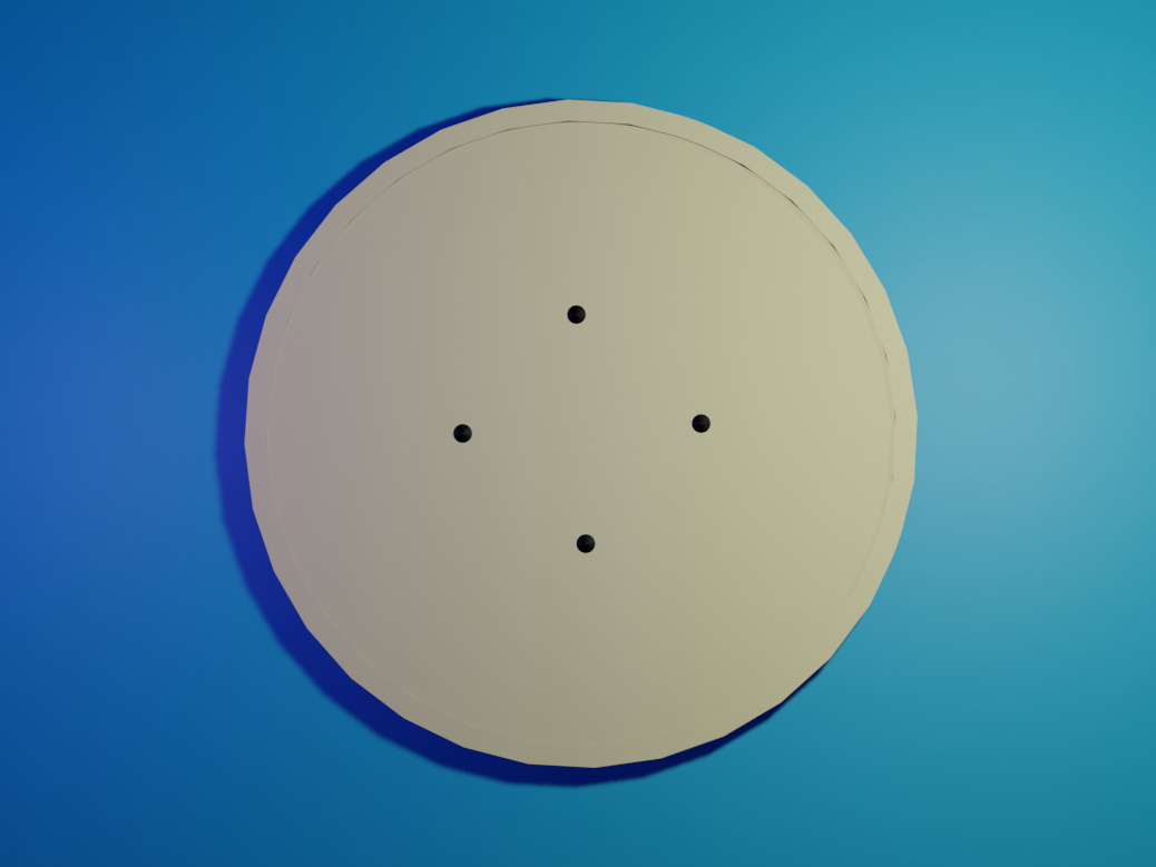
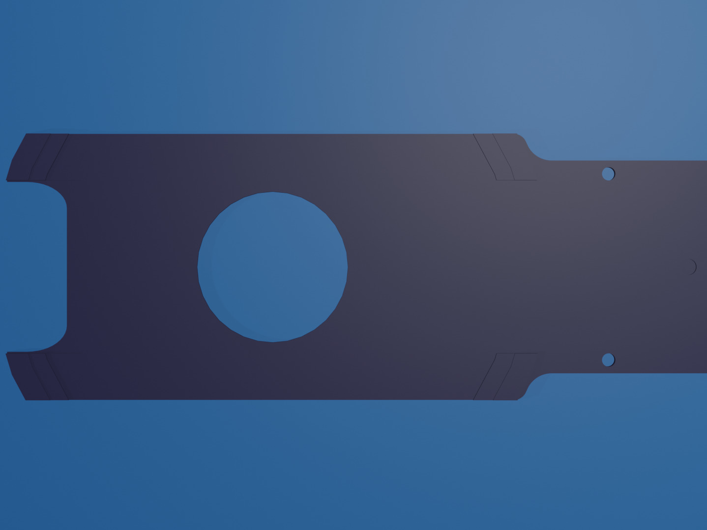
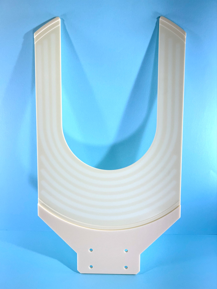
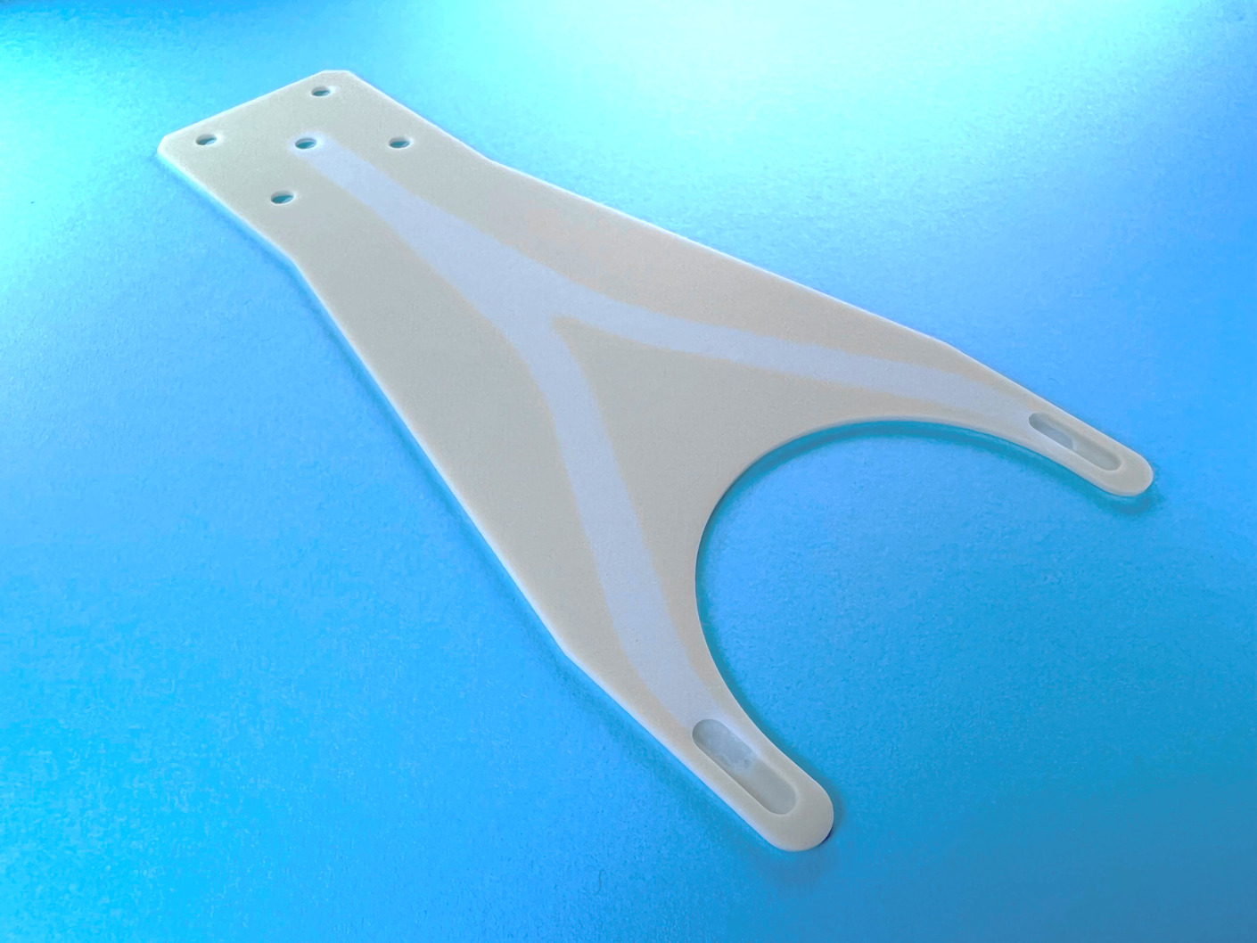
Product TypeWafer Transfer End Effector / Handling Arm
Customer's concerns and problems / Before
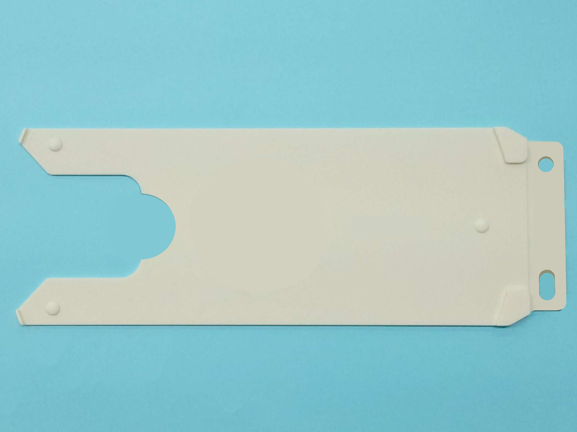
Our proposals and improvement effects / After
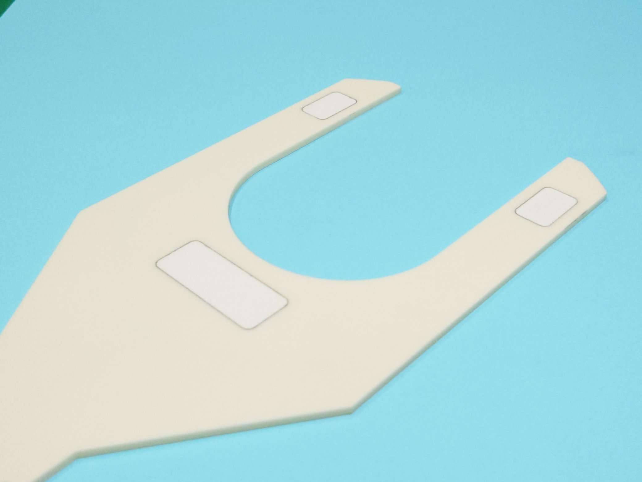
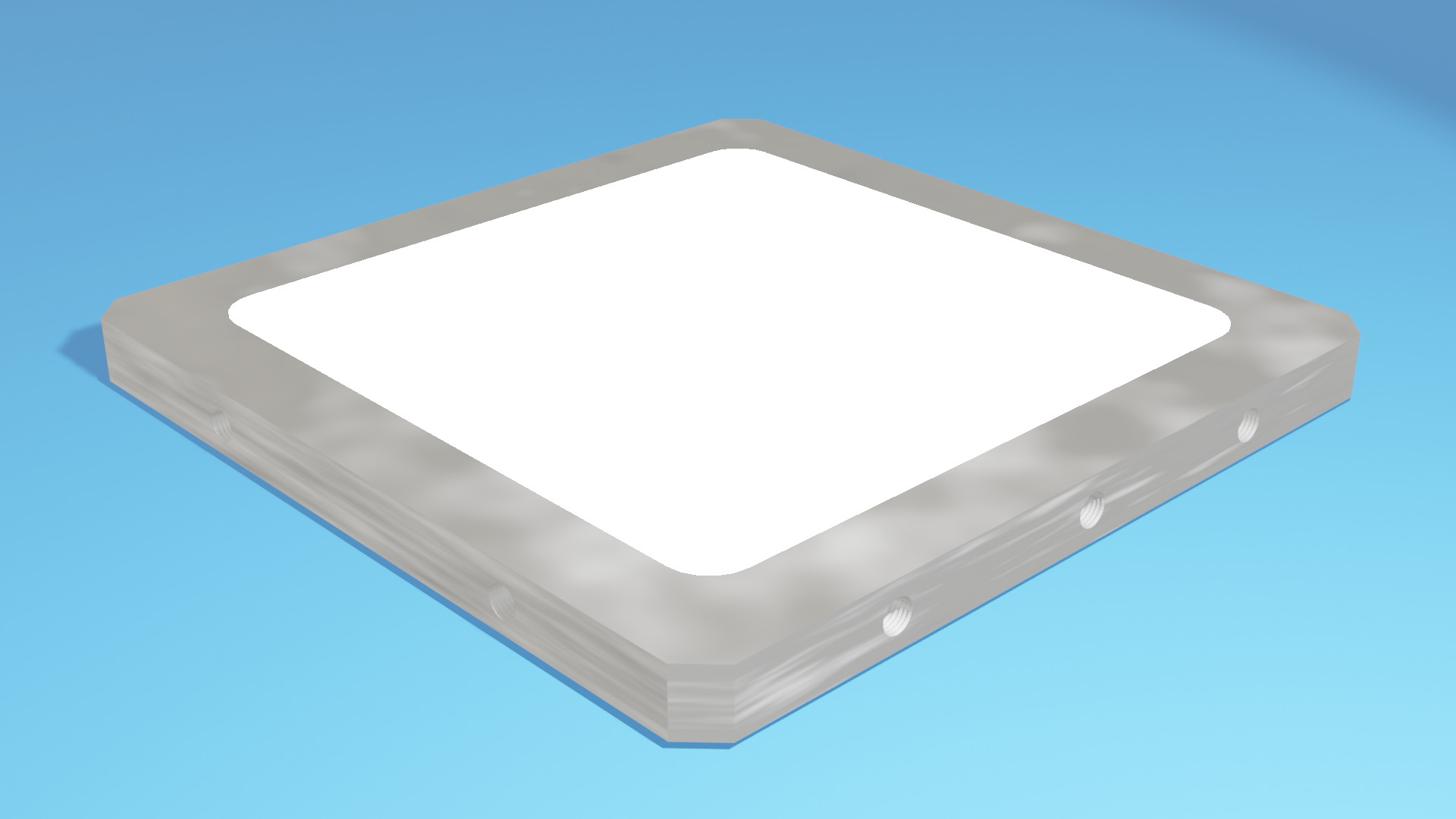
そこで「セラミックスデザインラボ」では、薄く反りのあるウエハを安定的に保持でき、ウエハへの傷や吸着痕を抑制できる多孔質埋め込みハンド(多孔質AZPV60、本体AR-99.6)をご提案いたしました。
その結果、ウエハ保持不足・バキュームリークによる薄反りウエハの破損や、ウエハの傷・吸着痕を低減することができ、歩留まり向上を実現いたしました。
Point of the proposed example / Point
本事例のポイントは、薄く反りのあるウエハを安定して保持し、且つウエハの傷や吸着痕を低減できた点にあります。
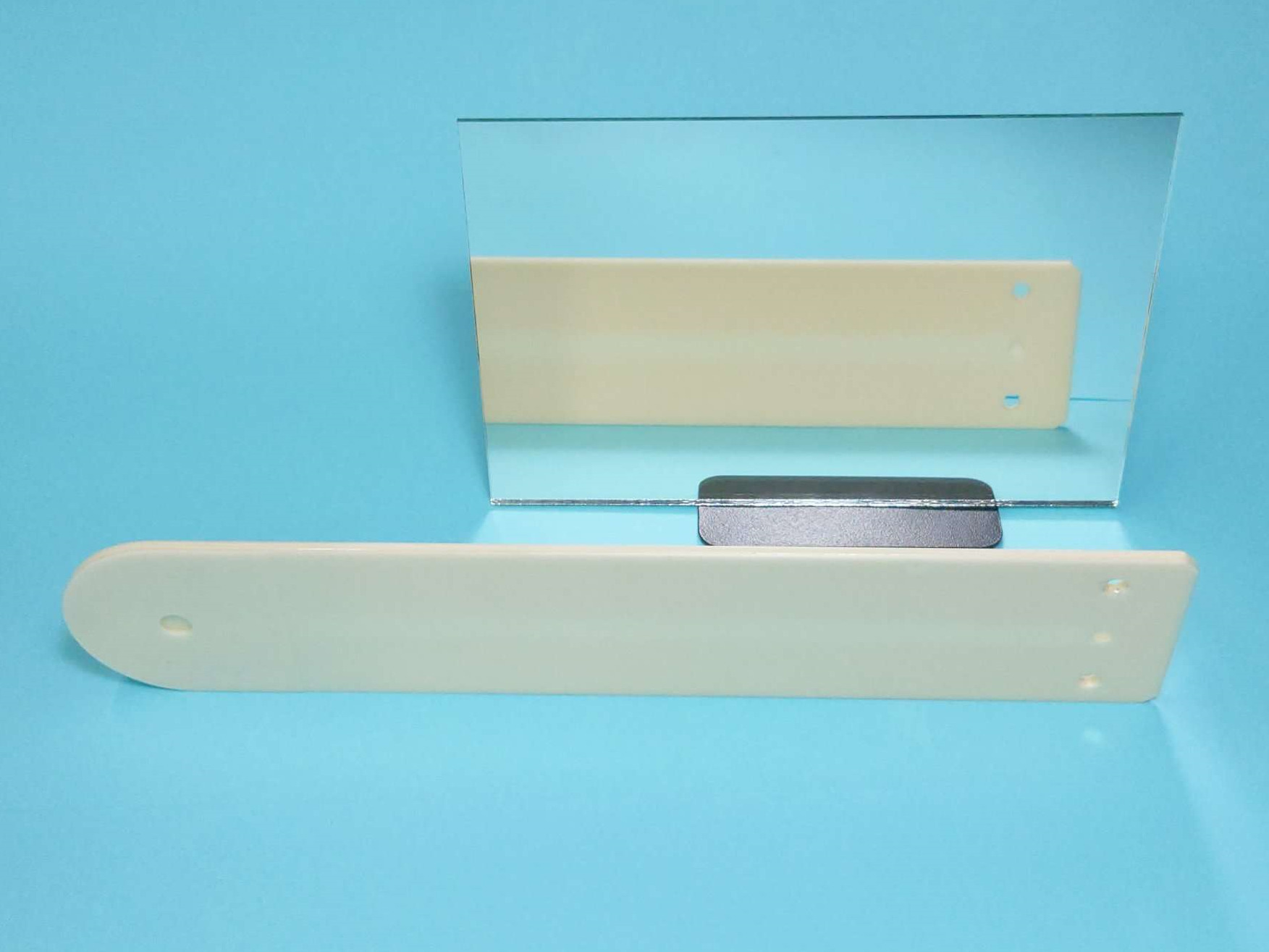
多孔質セラミックスAZPV60は、気孔径が40 μmと小さく、通気率が高いことが特徴です。薄く反ったウエハの吸着に向いています。フラットな面で均一に吸着するため、変形が起きにくいです。
「セラミックスデザインラボ」を運営するアスザック株式会社ファインセラミックス事業部では、材料開発・調合から、設計・製作、表面処理・検査・洗浄まで一貫対応しております。セラミックス材料に機能性を付加する独自のコーティング技術や、耐熱性・導電性をもつセラミックス材料、純度が高くコンタミを防げる高純度のアルミナ・SiCなどの材料選定についてもご提案させていただくことが可能です。薄く反りのあるウエハの搬送についてお困りの方やウエハの傷や吸着痕についてお困りの方は、お気軽にご相談ください。
Integrated response from processing to development of ceramic materials !
Please feel free to contact us !
TEL +81-26-248-1626
Business hours: 9:00-17:00 (closed on Saturdays, Sundays and Holidays)


.jpg)


.jpg)


半導体デバイスメーカーのお客様より、「露光工程において、薄く反ったウエハを搬送する際、吸着力不足によりウエハがうまく保持できないことがあります。また、ウエハへの傷や吸着痕にも困っています。何か良いハンドを提案をしていただけないでしょうか?」ということで、搬送ハンドの製作実績が豊富な当社にお問い合わせがありました。