-
ProblemsOutgassing
Heat Resistance
Conductivity
Static Electricity -
Proposed EffectImproved Heat Resistance
Anti-Static Measures
Surface Resistance Control
Outgassing Reduction -
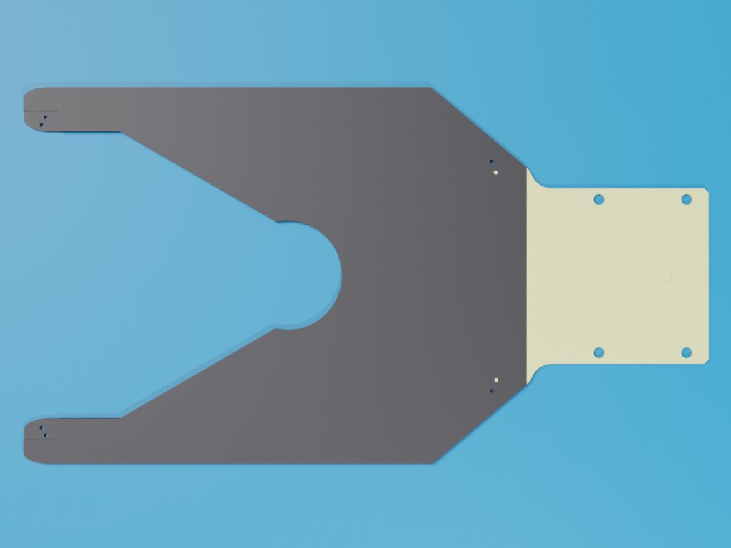
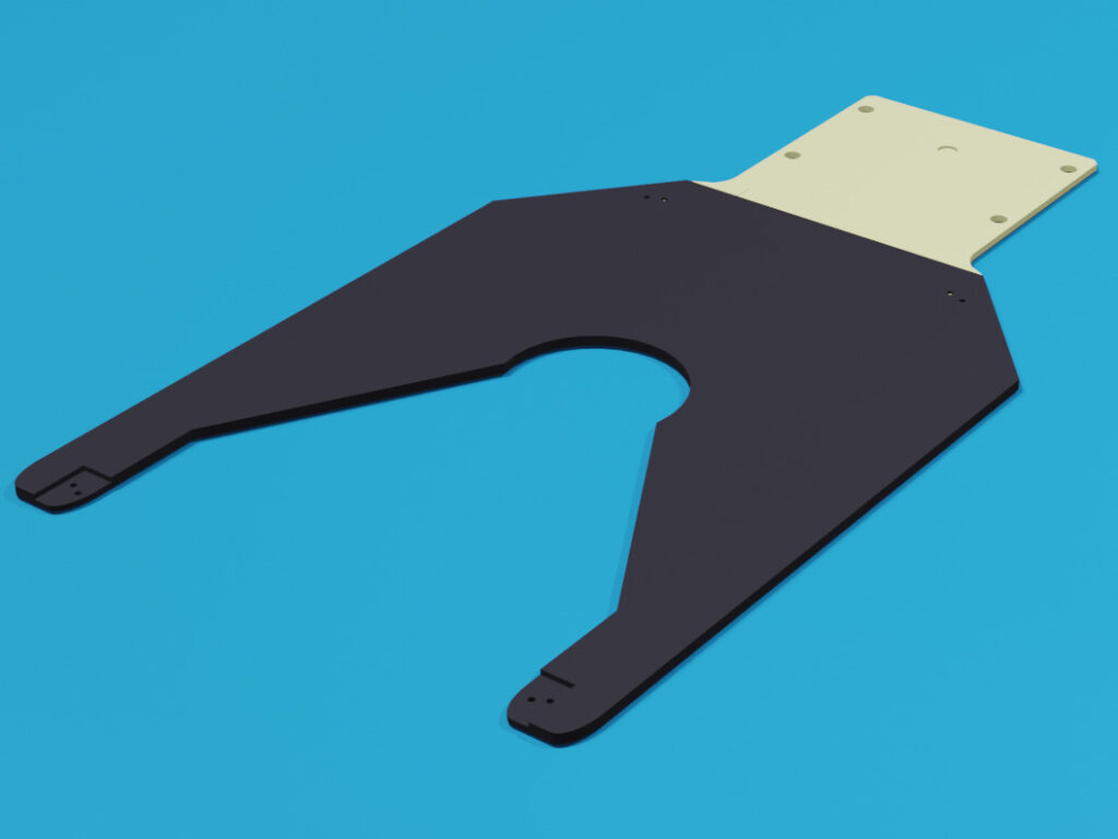
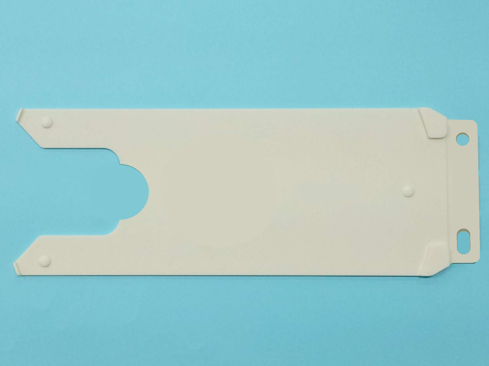
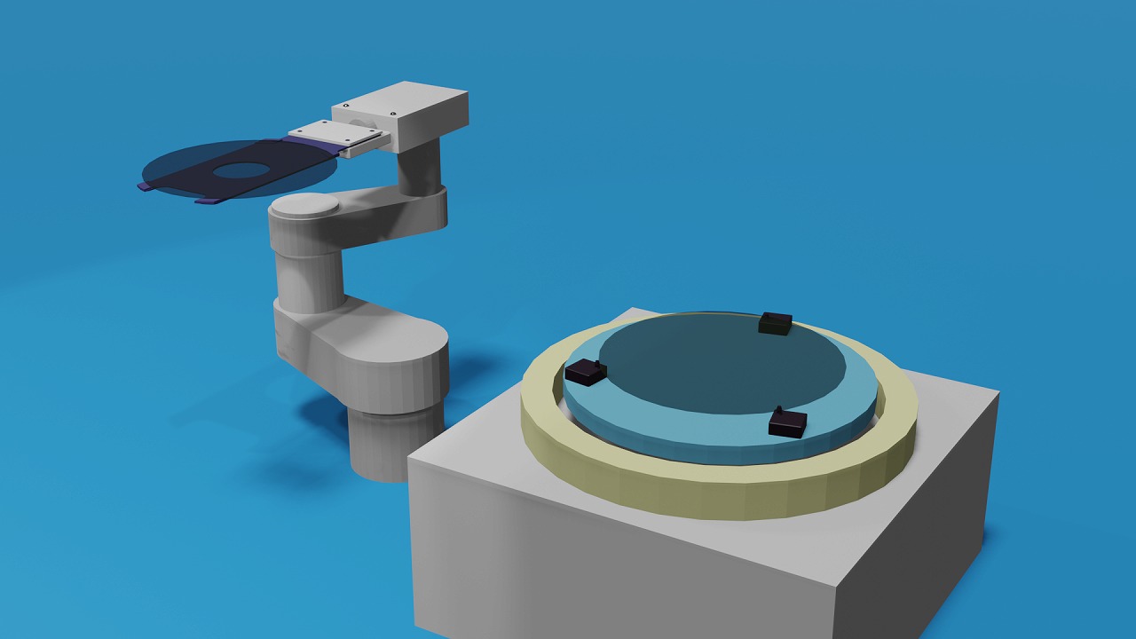
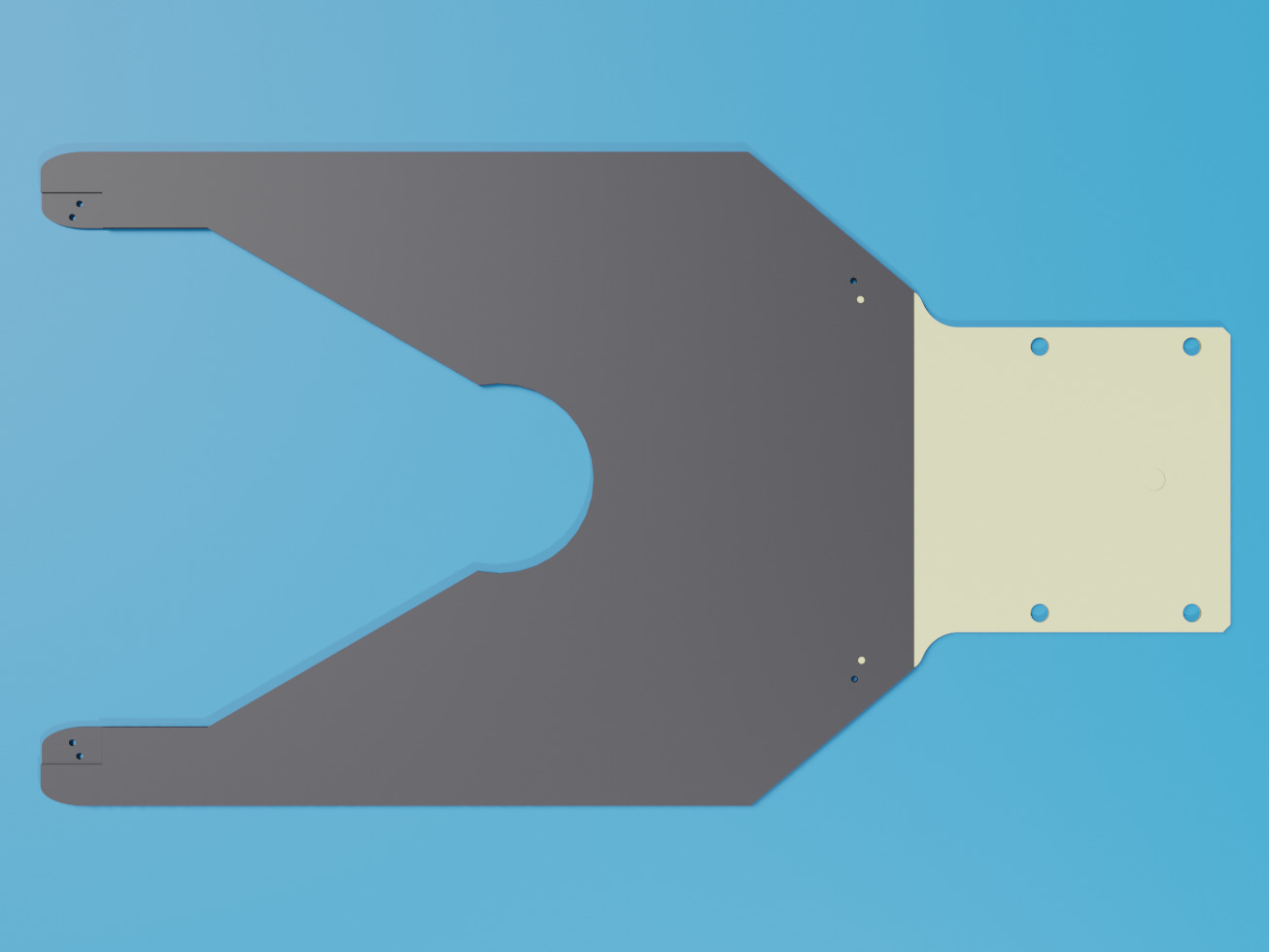
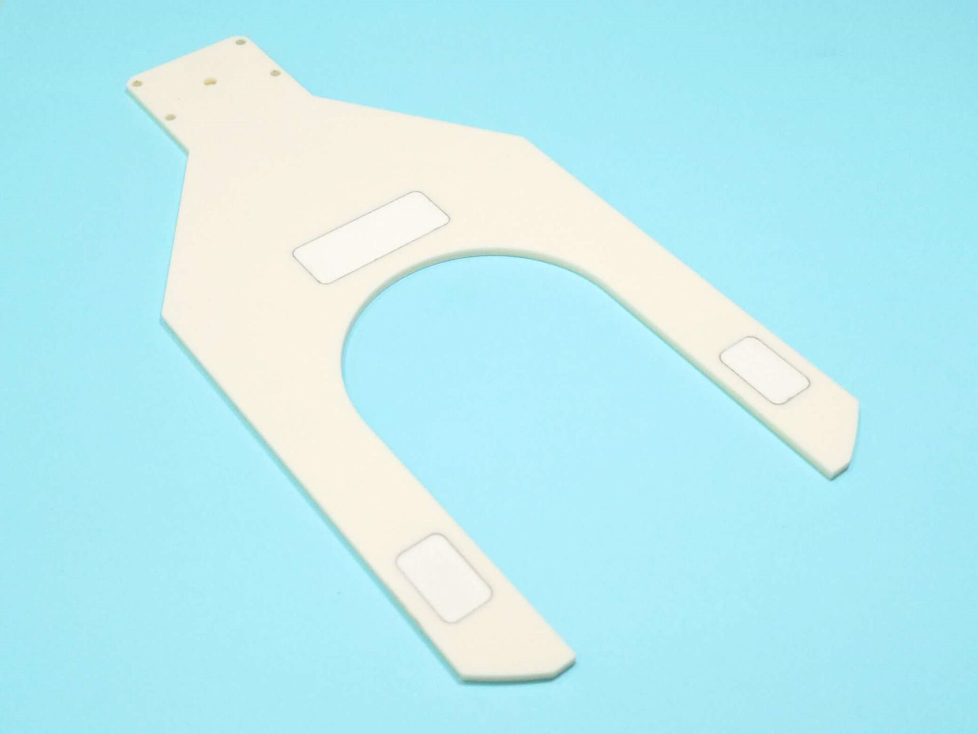
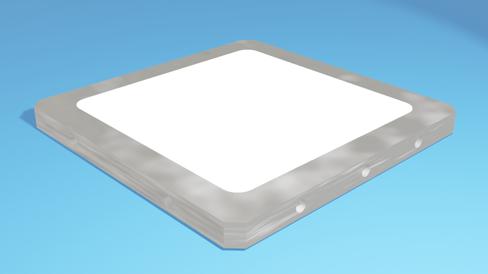
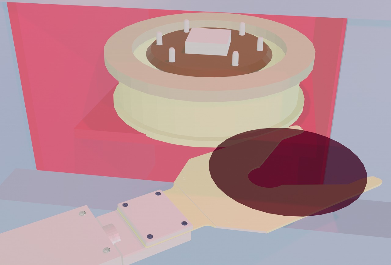
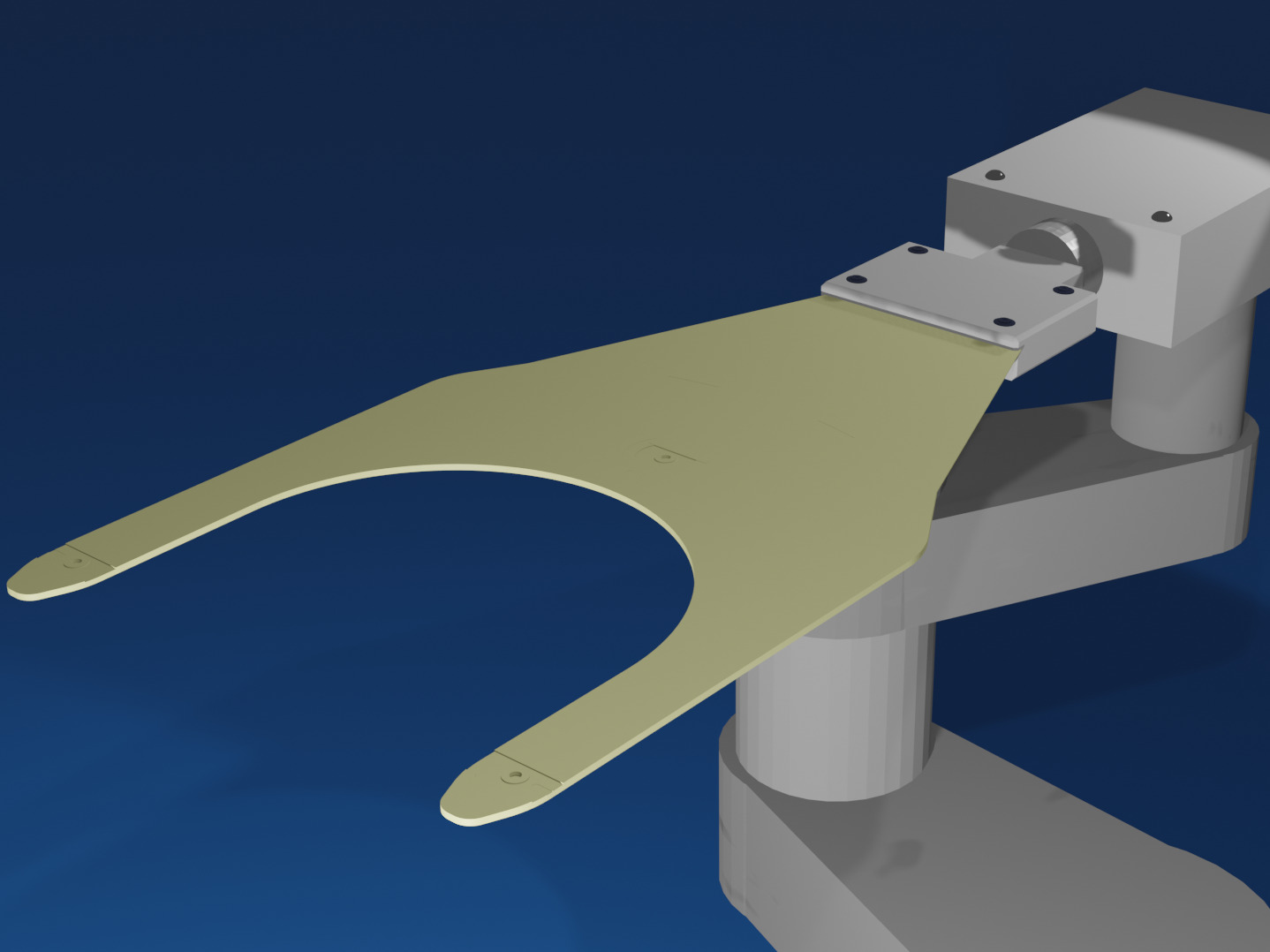
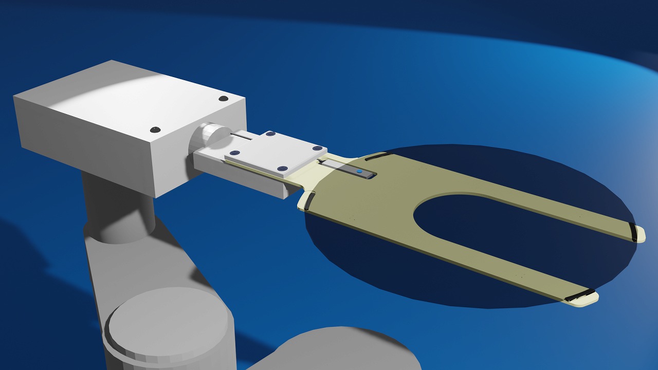
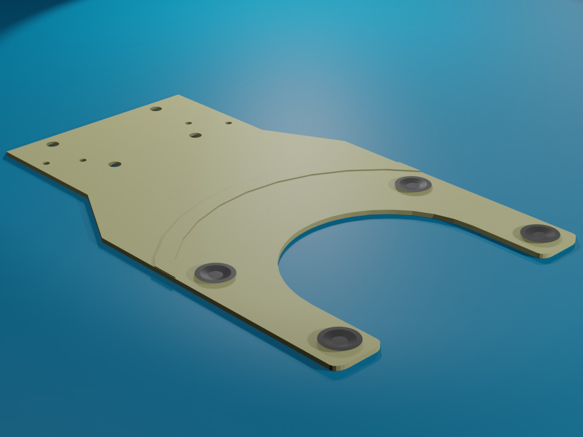
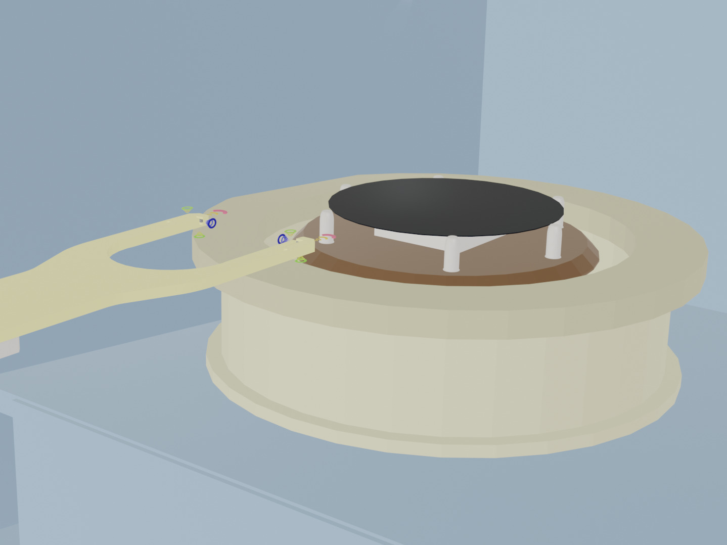
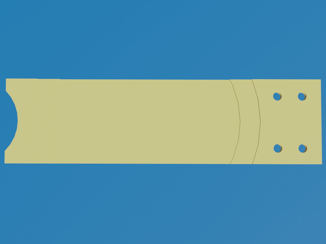
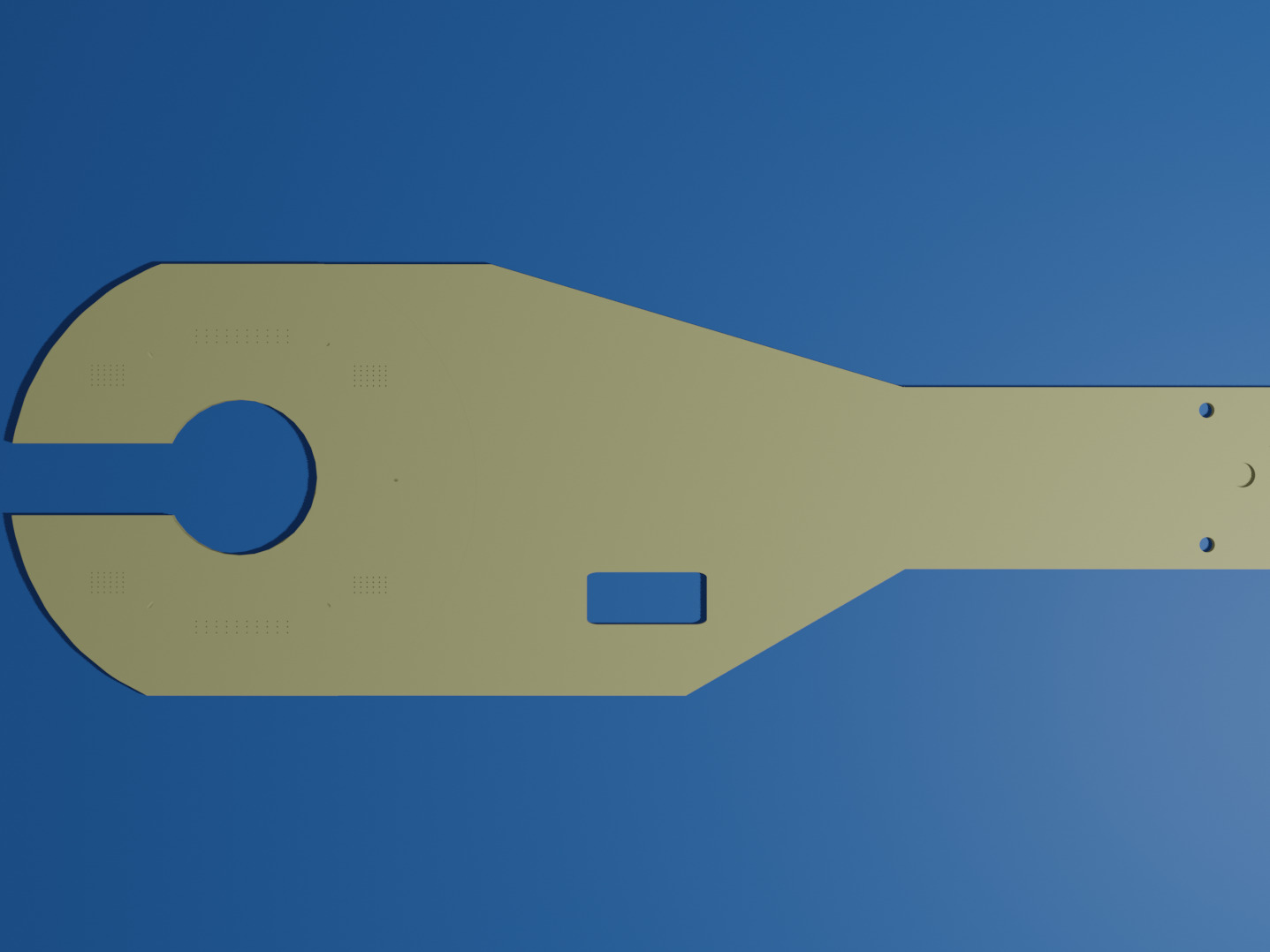
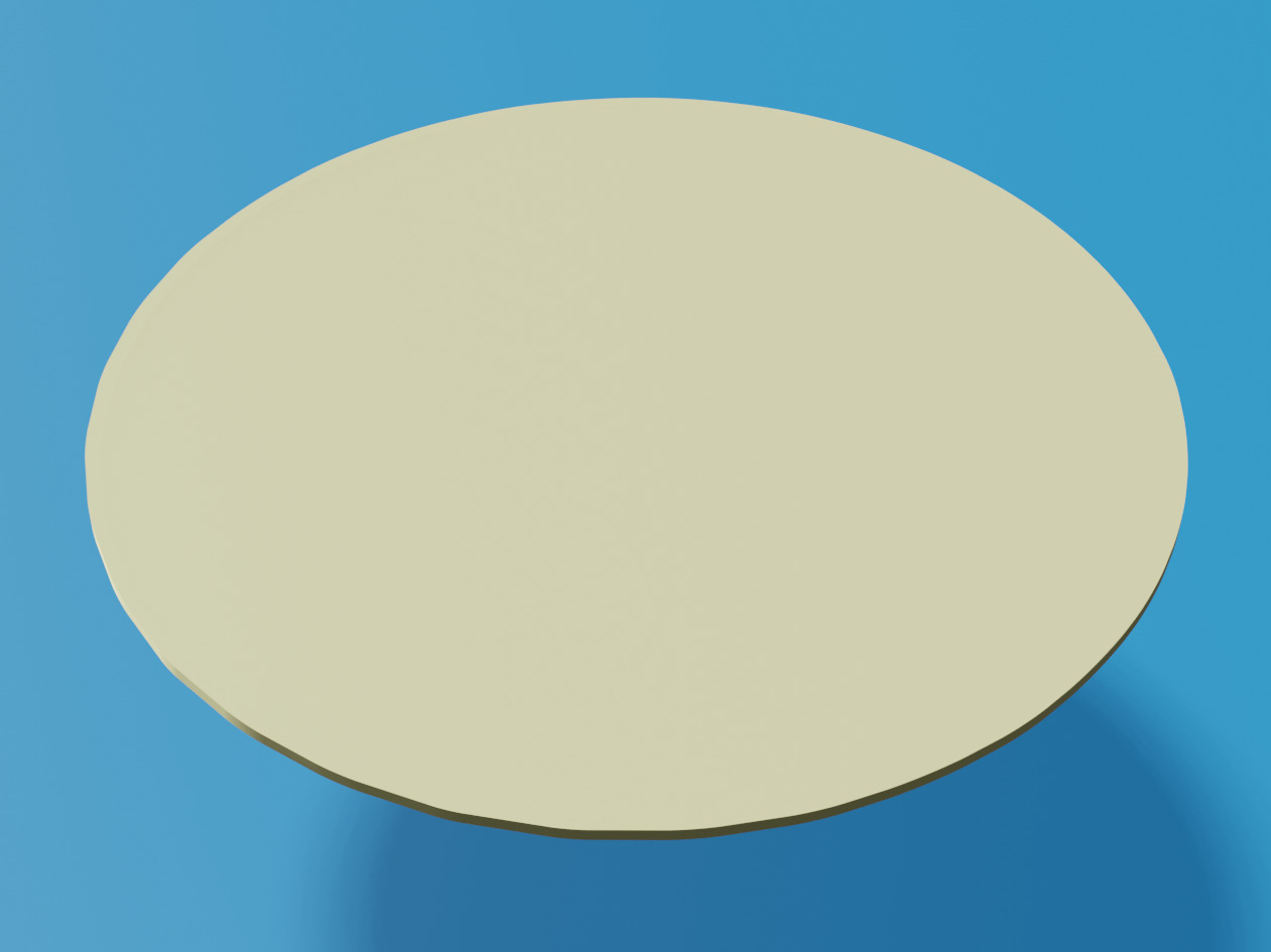
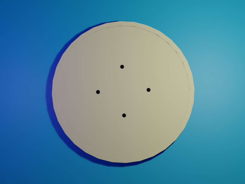
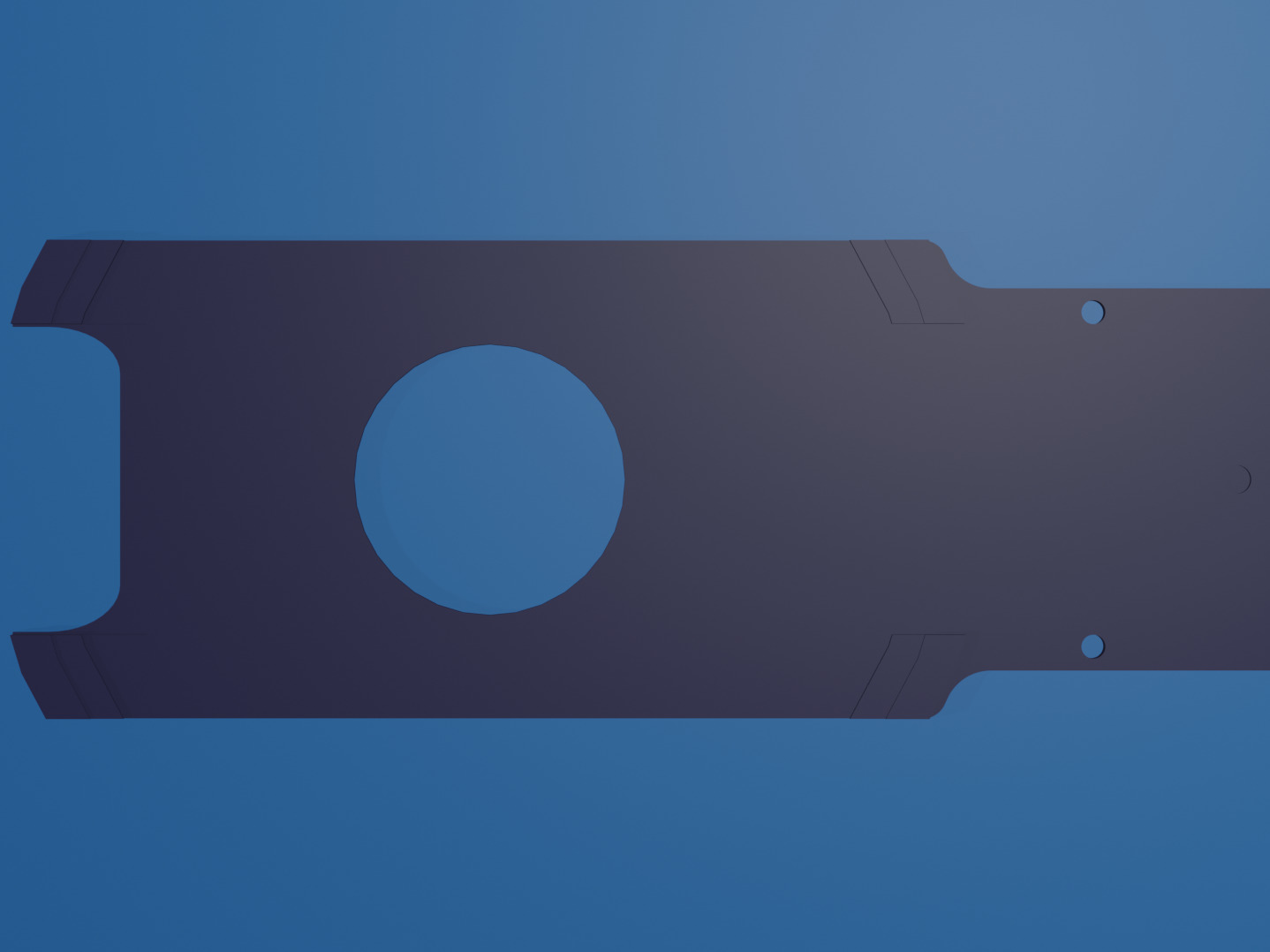
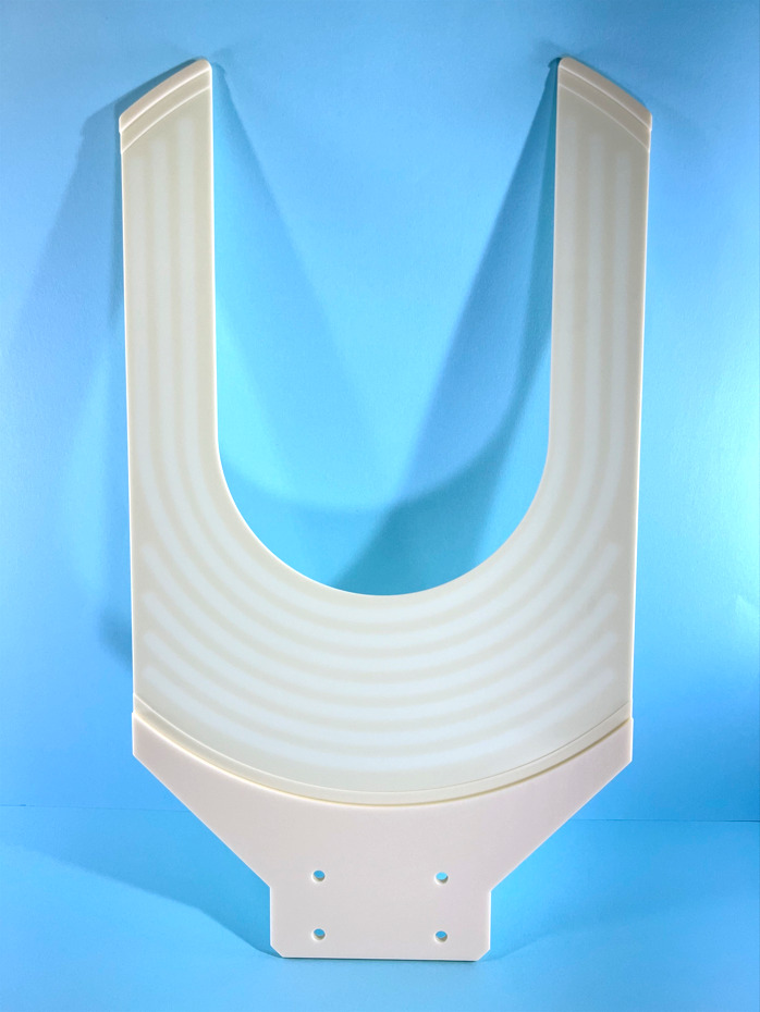
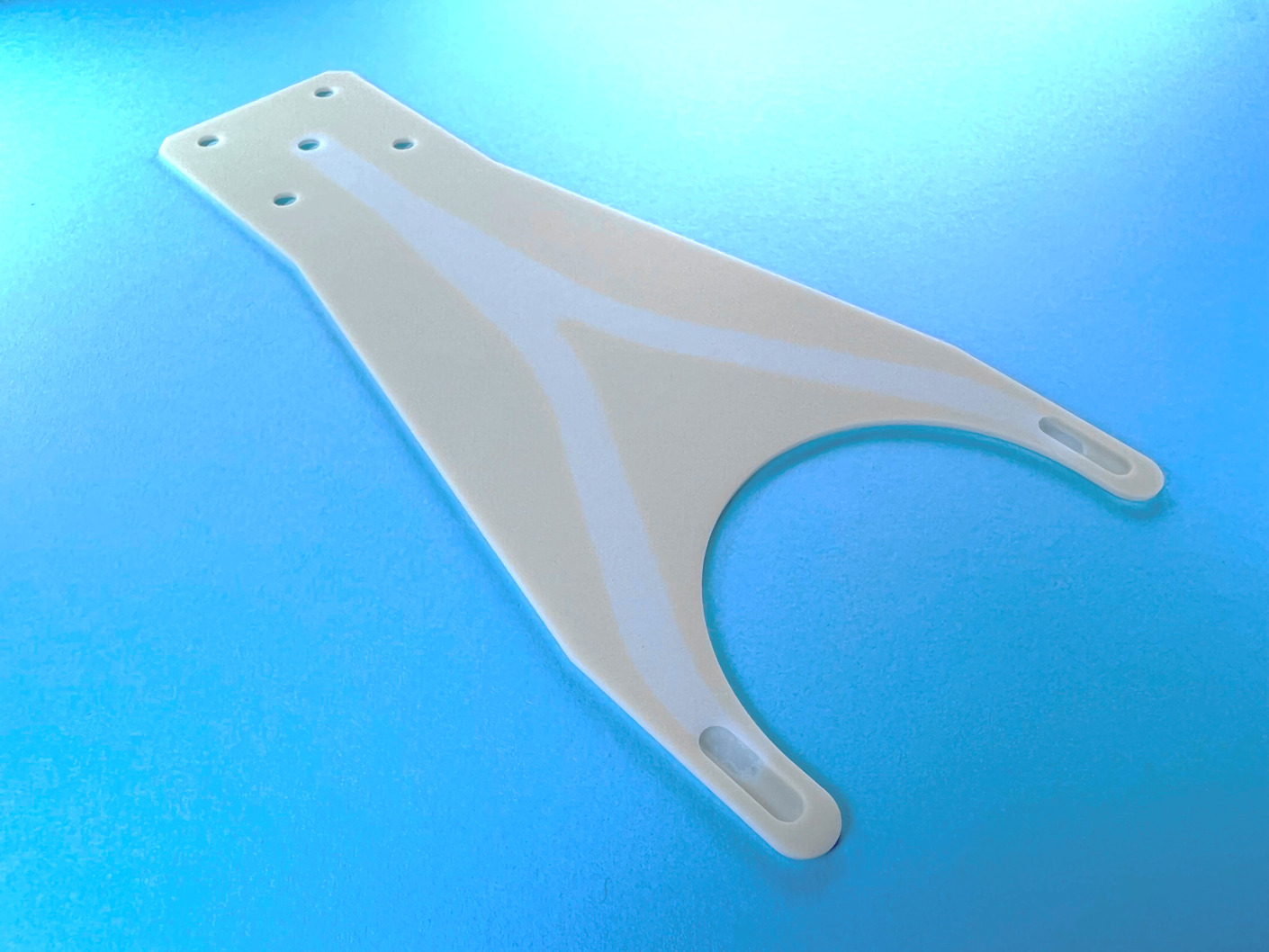
Product TypeWafer Transfer End Effector / Handling Arm
Customer's concerns and problems / Before
Our proposals and improvement effects / After
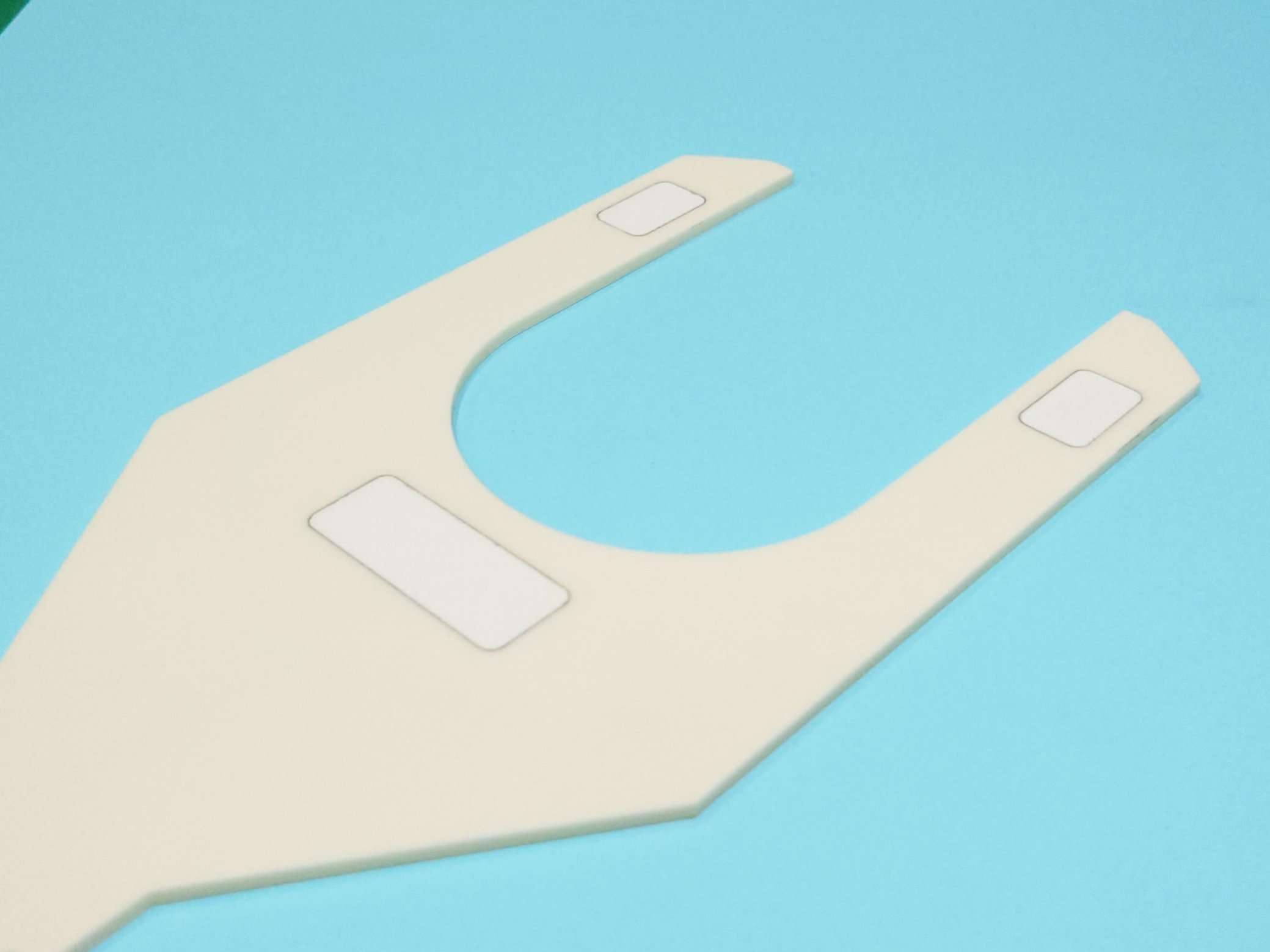
We proposed and evaluated ADB film, our original coating. We were able to satisfy all the requirements.
ADB film has a low surface-resistance even at high temperatures and is electrostatically dissipative.
It is also highly durable and can be used continuously for a long time.
With little outgassing, we were able to safely use it in new processes.


Point of the proposed example / Point
The point of this case is that the optimum selection of coating facilitates adaptation to new process environments.
Asuzac constantly develops state-of-the-art ceramics technologies, particularly in the semiconductor manufacturing industry, and offers solutions for issues such as outgas countermeasures.
The Fine Ceramics Division of ASUZAC Corporation, which operates the Ceramics Design Laboratory, handles everything from material development and preparation to design and manufacture, as well as surface treatment, inspection, and cleaning.
We can also offer our own coating-technology for adding functionality to ceramics materials, as well as the selection of materials such as ceramics materials with high heat resistance and conductivity, and high-purity alumina and SiC that are highly pure and prevent contamination.
If you have trouble with the existing wafer Transfer End Effector / Handling Arm, please feel free to contact us.
Integrated response from processing to development of ceramic materials !
Please feel free to contact us !
Business hours: 9:00-17:00 (closed on Saturdays, Sundays and Holidays)


.jpg)


.jpg)


In the newly developed process, no outgas was generated under high temperatures, and a conductive transport End Effector / Handling Arm was required.
There was concern about outgas from the viewpoint of the coating material in the conventional conductive fluororesin coating specifications, but we did not find a suitable coating in many cases.