-
ProblemsHeat Resistance
Static Electricity
Surface Resistance -
Proposed EffectImproved Functionality
Anti-Static Measures
Surface Resistance Control -
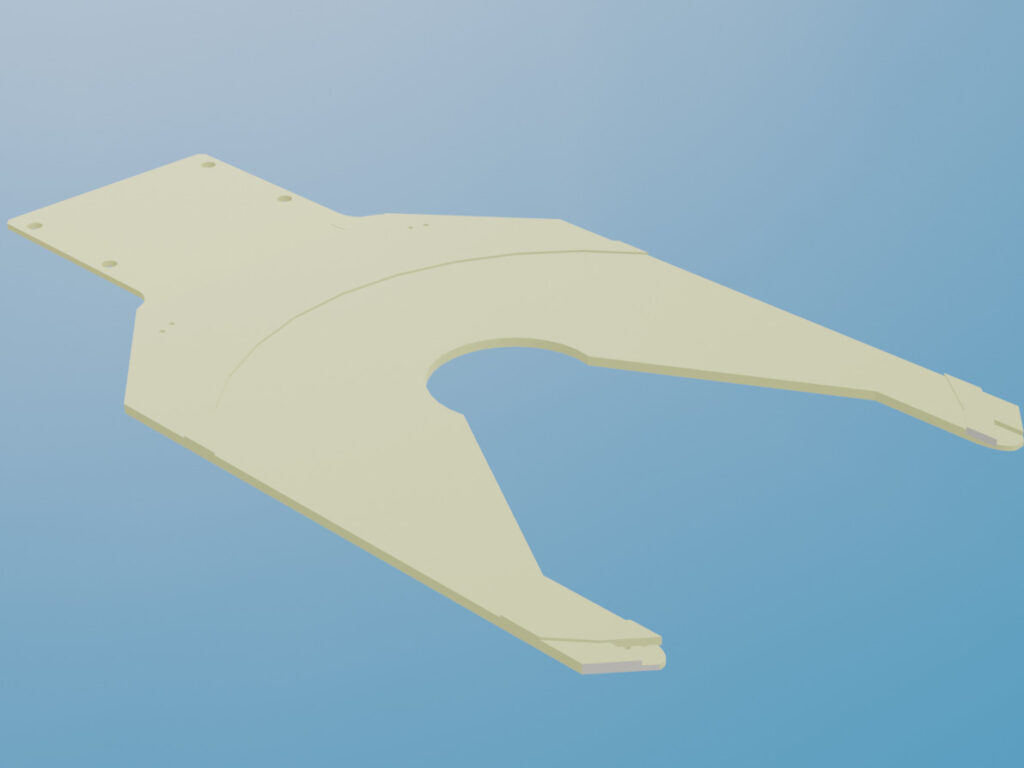
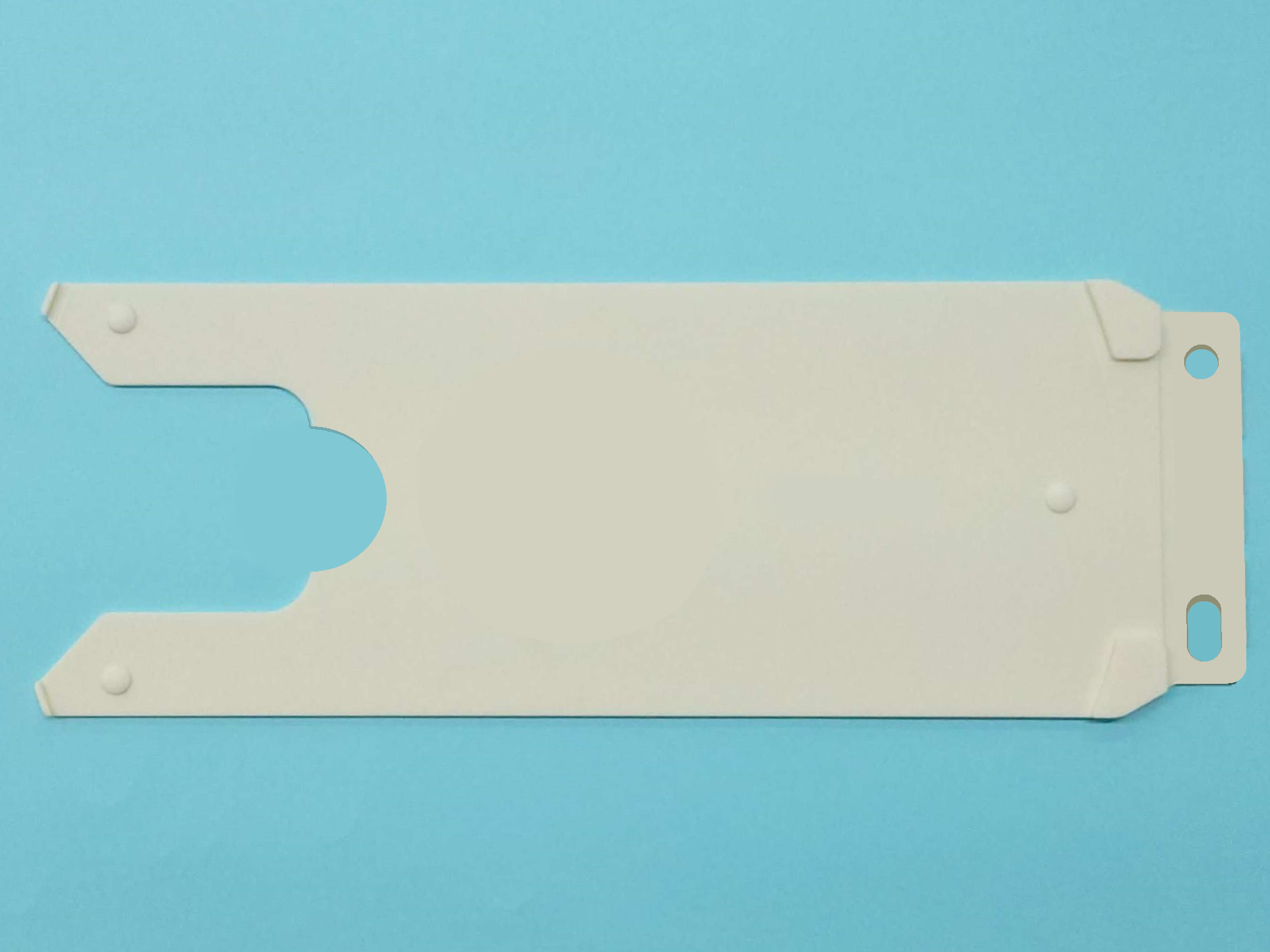
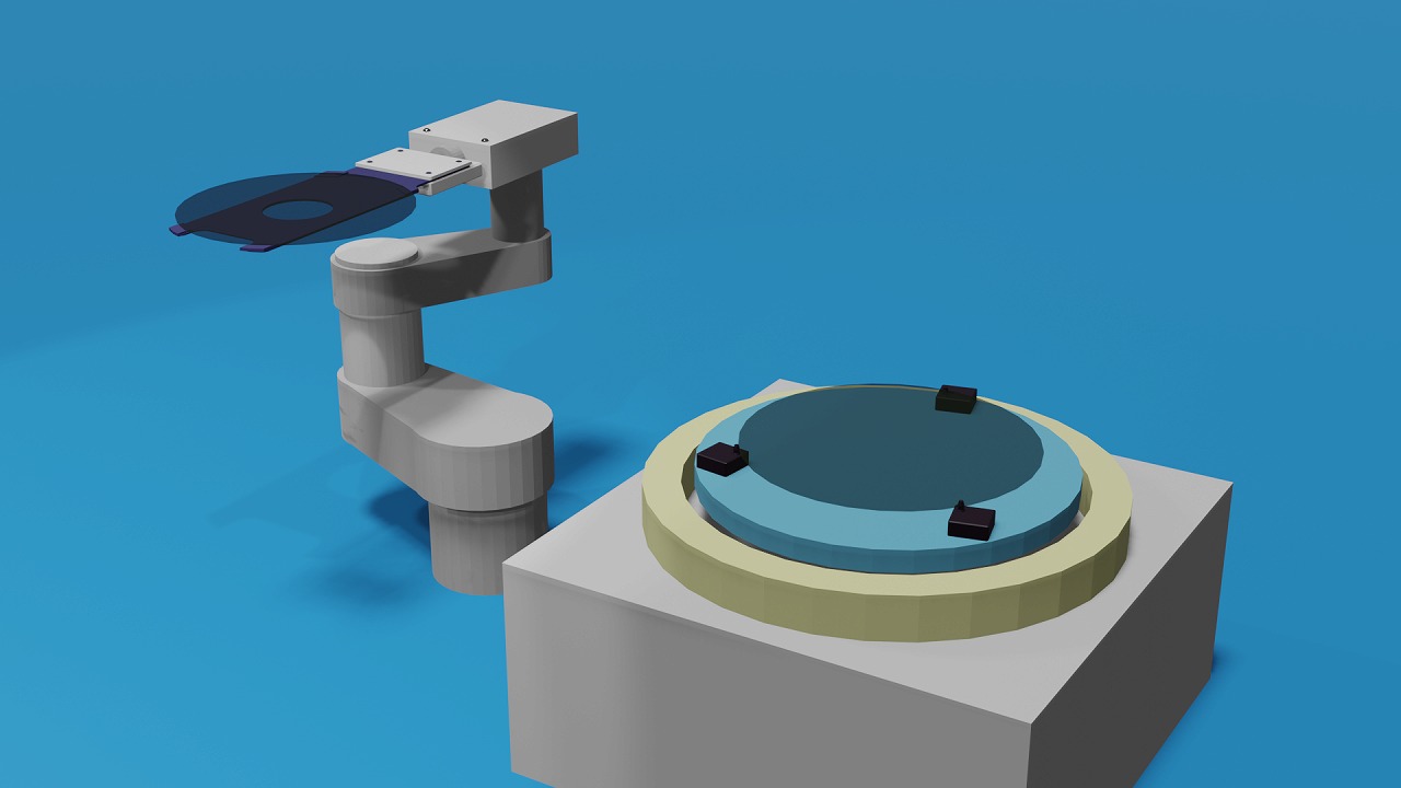
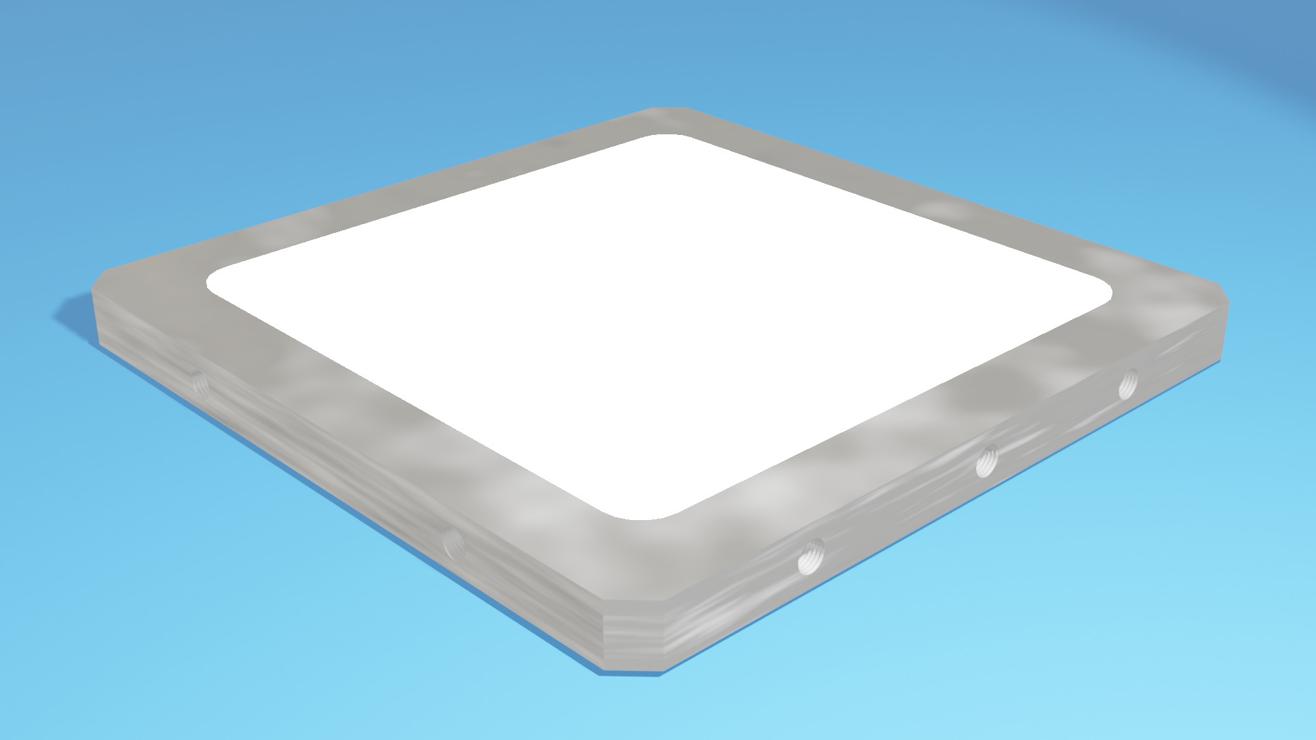
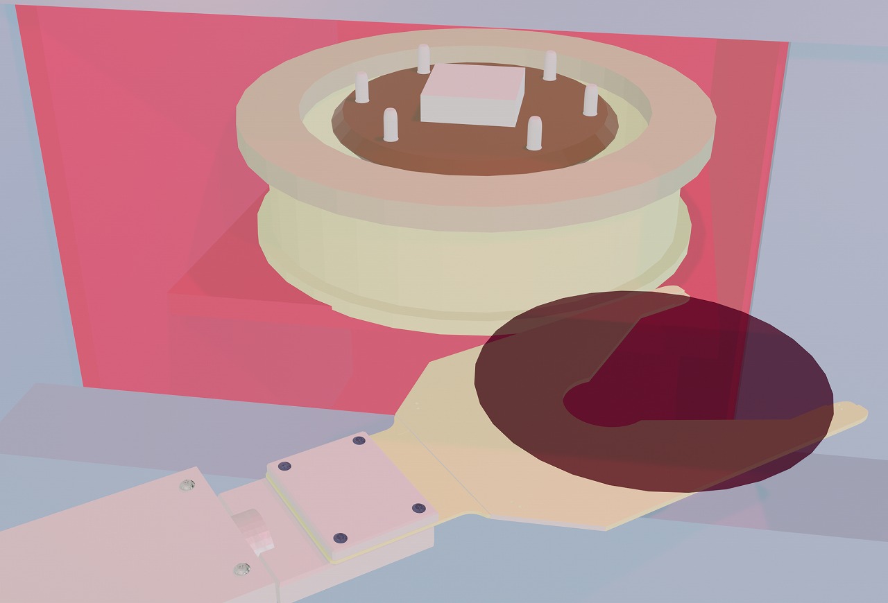
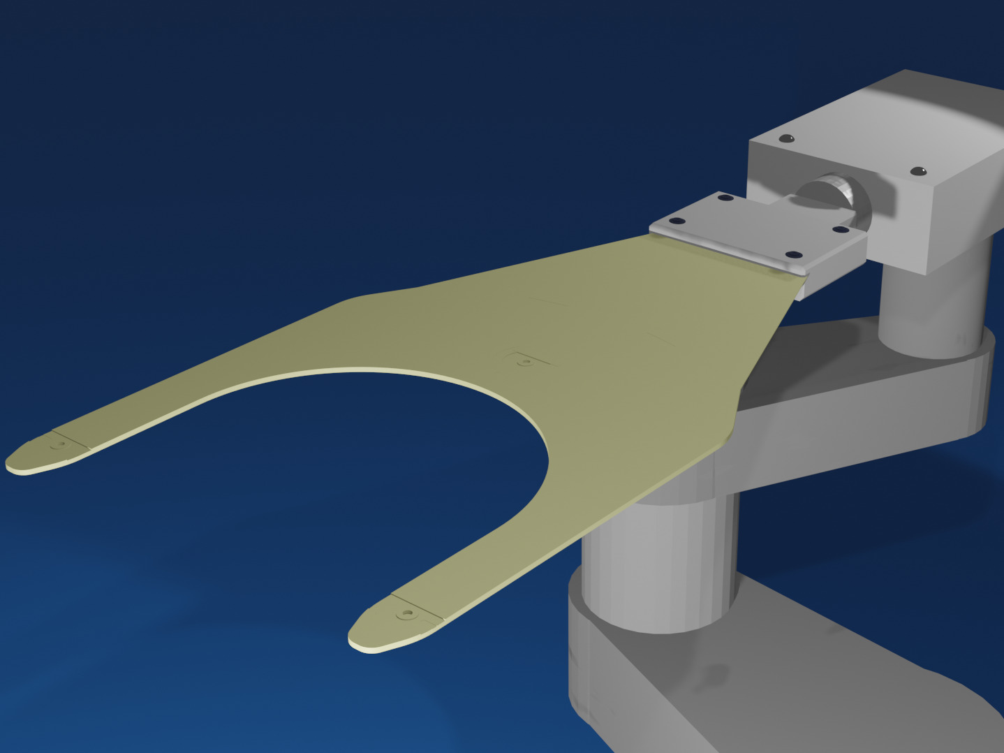
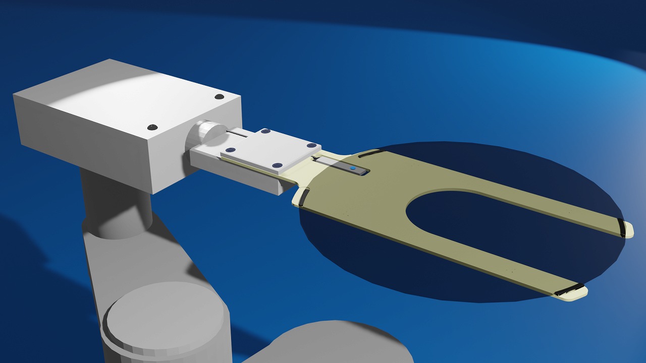
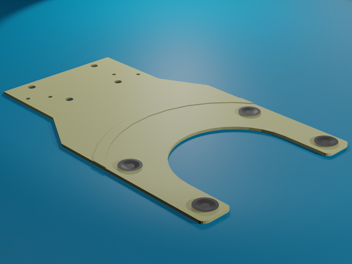
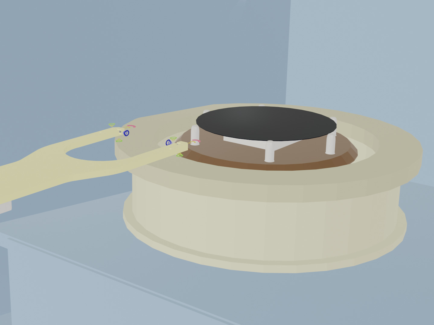
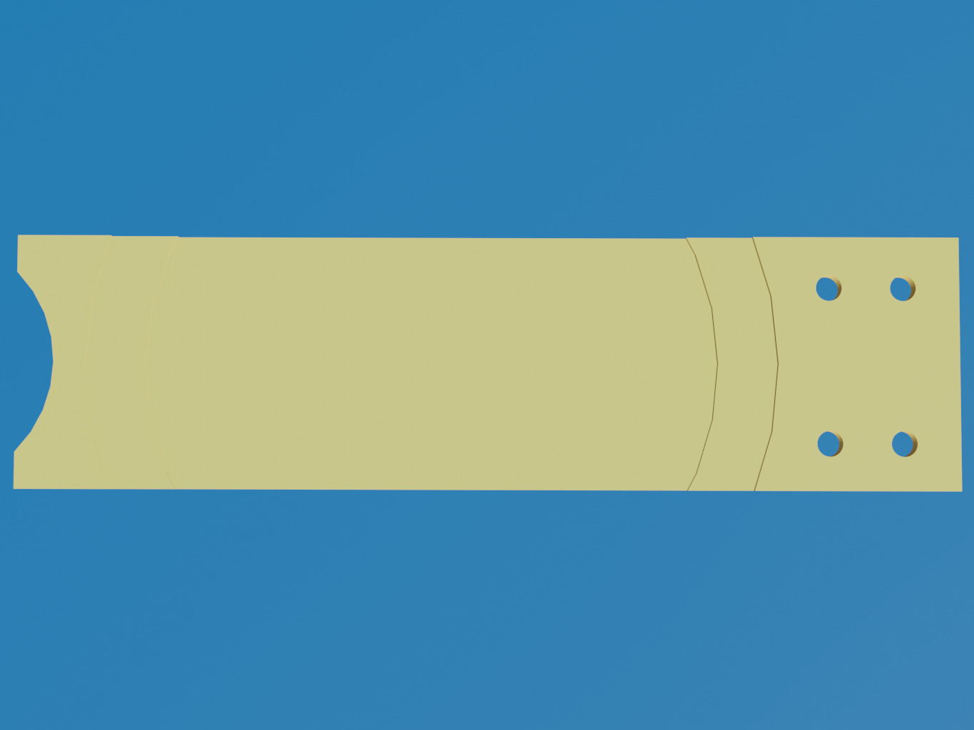
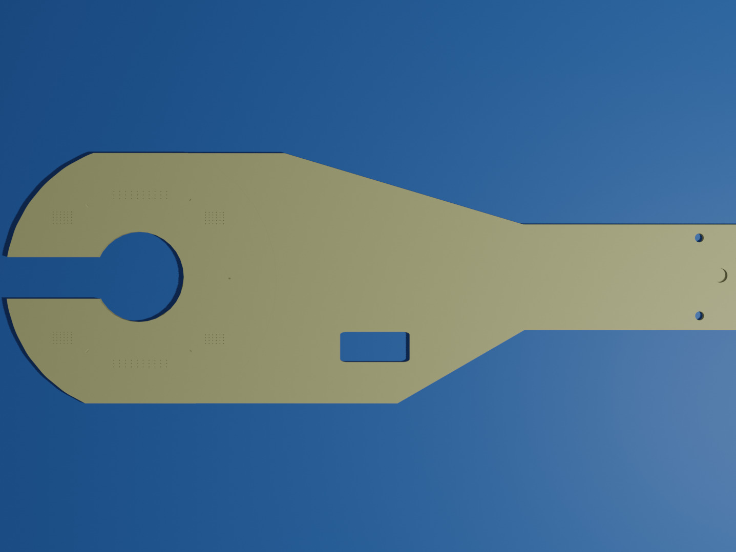
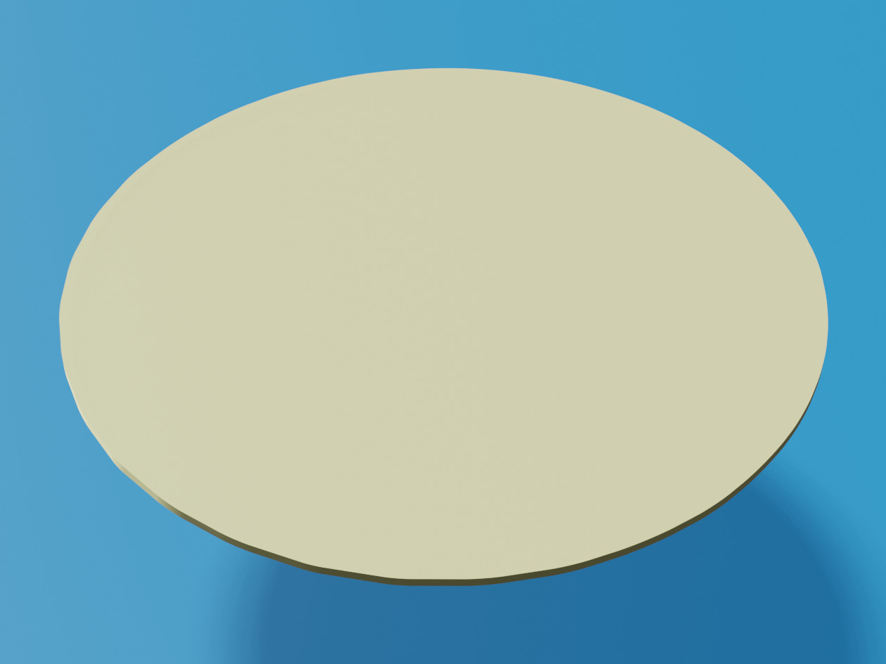
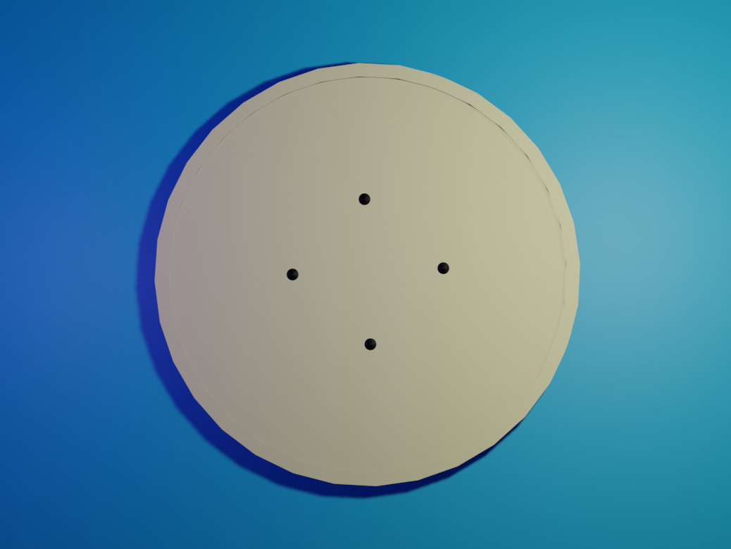
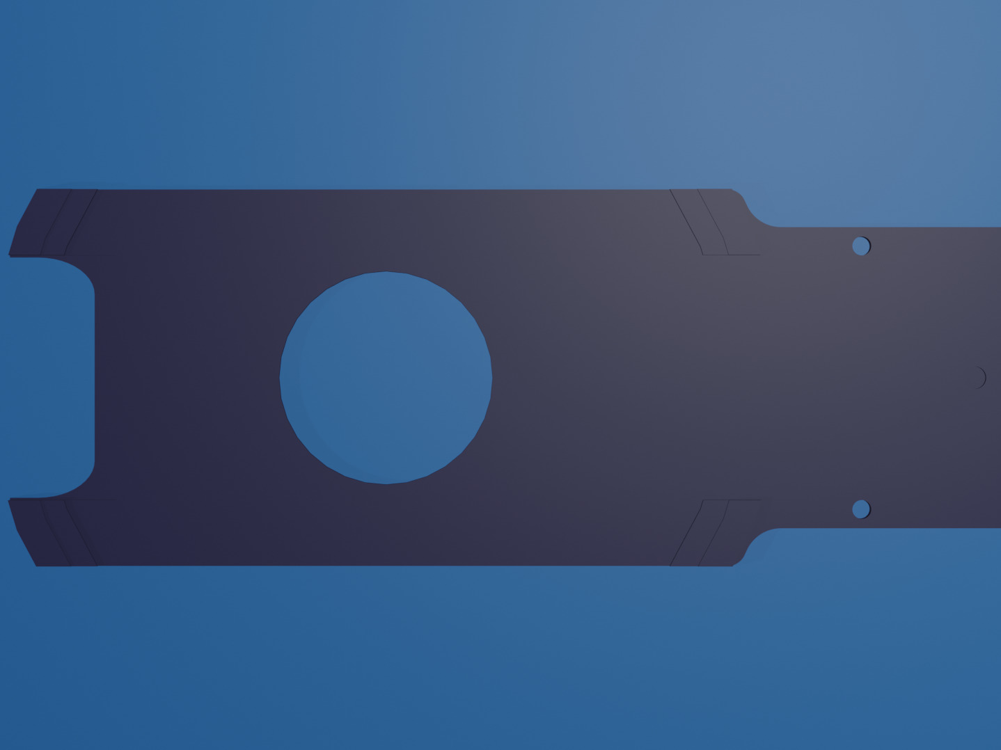
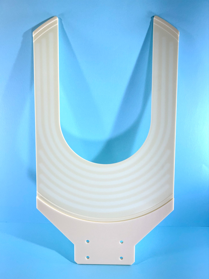
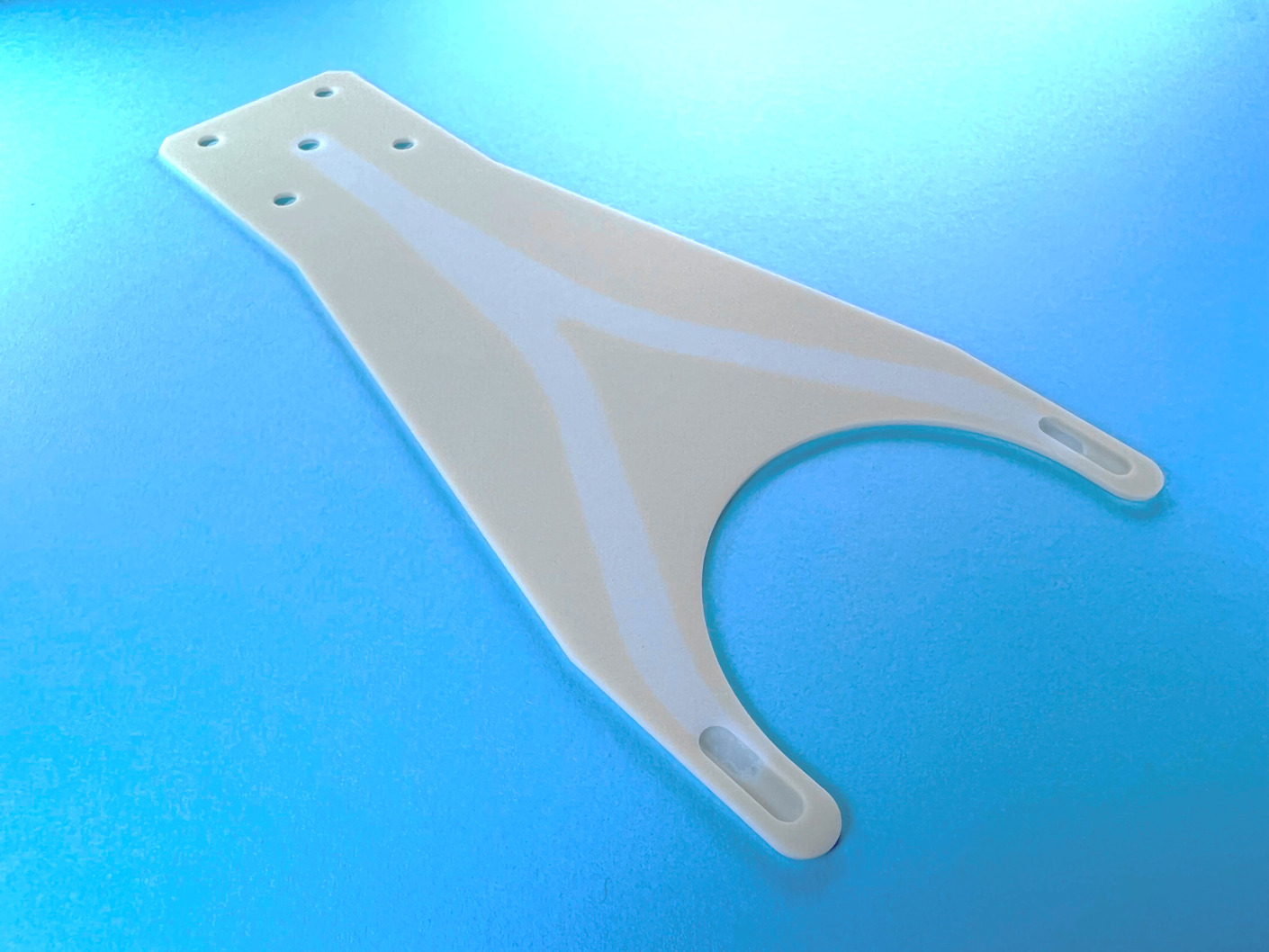
Product TypeWafer Transfer End Effector / Handling Arm
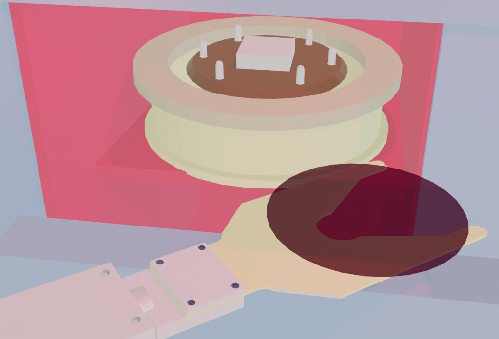
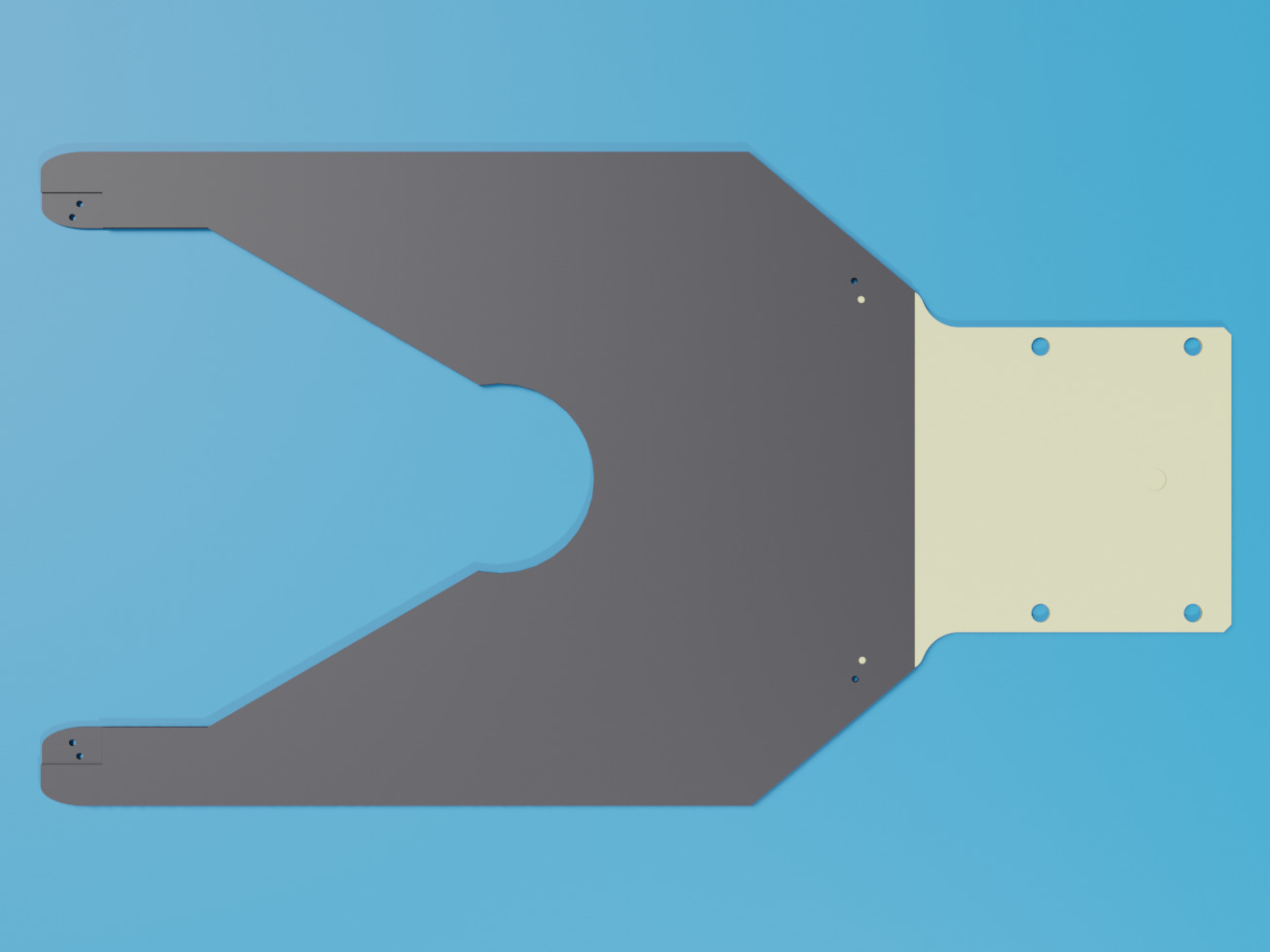
Customer's concerns and problems / Before
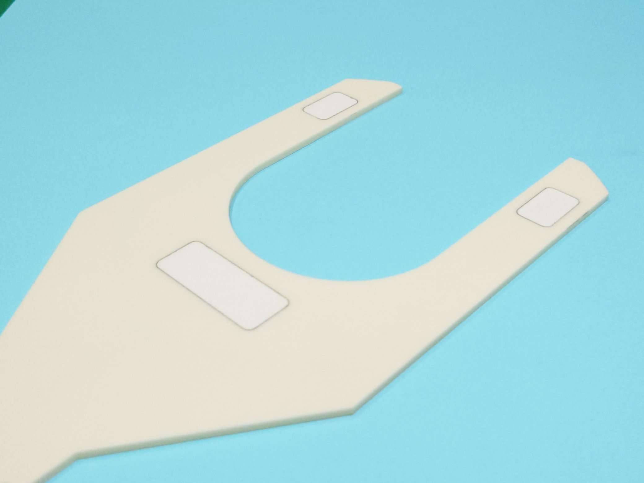
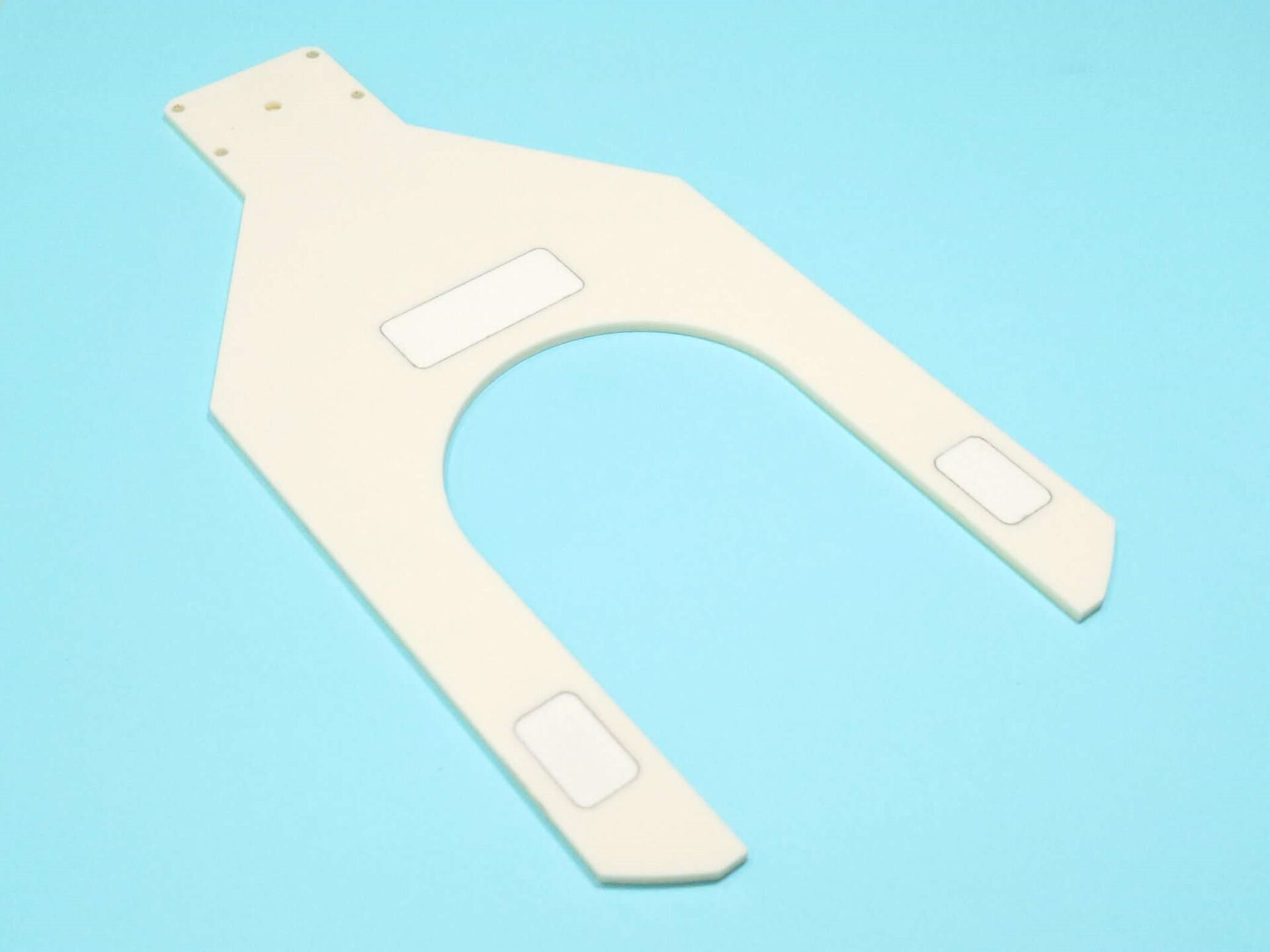
Our proposals and improvement effects / After
Therefore, the Ceramics Design Laboratory proposed a wafer Transfer End Effector / Handling Arm with our original coated “ADC film” that has a low surface-resistance even at high temperatures and is highly effective in diffusing static electricity.
As a result of actual use by customers, they said that they could be used in high-temperature environments at 500 ℃ to 750 ℃ without any problems.

Point of the proposed example / Point
The point of this case is that a special coating realizes a wafer Transfer End Effector / Handling Arm with a low surface resistance value and high electrostatic diffusion effect even under high temperature.
Electrostatic diffusivity is very important in preventing lint from adhering to the surface of the wafer when it is wiped off with a waste cloth or in taking measures against particles.
Our proprietary coating-technology ADC film maintains a low-surface-resistance even in high-temperature environments, ensuring sufficient electrostatic diffusivity.
The Fine Ceramics Division of ASUZAC Corporation, which operates the Ceramics Design Laboratory, handles everything from material development and preparation to design and manufacture, as well as surface treatment, inspection, and cleaning.
We can also offer our own coating-technology for adding functionality to ceramics materials, as well as the selection of materials such as ceramics materials with high heat resistance and conductivity, and high-purity alumina and SiC that are highly pure and prevent contamination.
If you are troubled by defects caused by lint or impurities, please feel free to contact us.
Integrated response from processing to development of ceramic materials !
Please feel free to contact us !
Business hours: 9:00-17:00 (closed on Saturdays, Sundays and Holidays)


.jpg)


.jpg)


From a customer of a semiconductor manufacturing equipment manufacturer, we consulted with us, who has an extensive experience in manufacturing wafer Transfer End Effector / Handling Arm, stating, “Is it possible to manufacture a wafer transfer Transfer End Effector / Handling Arm that can withstand 500°C to 800°C operating environment and has a sufficient electrostatic diffusion effect?”