Transfer End Effector / Handling Arm for semiconductors

We can solve your wafer transfer problems in semiconductor manufacturing and inspection processes!

CERAMICS DESIGN LAB > Transfer End Effector / Handling Arm for semiconductors

Are there any problems like this?

Transfer End Effector / Handling Arm for semiconductors|Ceramics Design Lab
  • We are looking for a transport End Effector / Handing Arm that can be used even in high-temperature environments...

  • I want to attach the sensor to the transfer End Effector / Handing Arm...

  • I want to replace metal transfer End Effector / Handing Arm with ceramics transfer End Effector / Handing Arm that are lighter in weight.....

Let us help you !

Integrated support from developing not only Alumina and SiC but also porous ceramics and special ceramics with excellent heat resistance and electrical conductivity!

We have a proven track record of production of various industries, applications, and shapes such as wafer transfer End Effector / Handling Arm, vacuum chucks, large boards, and firing setters!

We offer proposals for VA / VE to customers that are possible only because they are familiar with the characteristics of ceramic materials and the problems unique to the semiconductors and electronics industries!

If you are in a hurry, please call us!

TEL+81-26-248-1626

Business hours: 9:00-17:00 (closed on Saturdays, Sundays and Holidays)

This site "Ceramics Design Lab" is operated by the Fine Ceramics Division.
ASUZAC Corporation is a group founded in 1946 and
consisting of more than 800 people.

Characteristics of our "Transfer End Effector / Handling Arm for semiconductors"

  • Transfer End Effector / Handling Arm for semiconductors|Ceramics Design Lab

    We can solve your wafer transfer problems in semiconductor manufacturing and inspection processes!

    Our ceramics wafer transfer End Effector / Handling Arm are thinner and more durable thanks to our proprietary Ceramic Design Lab technology, an adhesive-free cavity-integrated technology.

    Ceramics materials have the advantages of: resistance to high-temperature environments, low risk of metal contamination and dust, and advantages in preventing organic outgassing.

    Our past achievements include the following.

    We have manufactured transfer End Effector / Handling Arm with different suction methods for the front and back surfaces with a single End Effector / Handling Arm , manufactured End Effector / Handling Arm for transferring PLP substrates of 500 square and 600 square sizes, and handled everything from custom-made wafer transfer End Effector / Handling Arm to evaluation tests.

Examples and Achievements of our "Transfer End Effector / Handling Arm for semiconductors"

Let us help you !

Integrated support from developing not only Alumina and SiC but also porous ceramics and special ceramics with excellent heat resistance and electrical conductivity!

We have a proven track record of production of various industries, applications, and shapes such as wafer transfer End Effector / Handling Arm, vacuum chucks, large boards, and firing setters!

We offer proposals for VA / VE to customers that are possible only because they are familiar with the characteristics of ceramic materials and the problems unique to the semiconductors and electronics industries!

If you are in a hurry, please call us!

TEL+81-26-248-1626

Business hours: 9:00-17:00 (closed on Saturdays, Sundays and Holidays)

Frequently Asked Questions on "Transfer End Effector / Handling Arm for semiconductors"

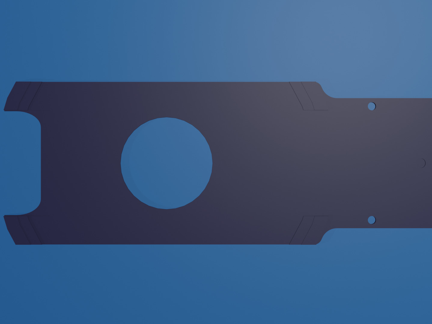
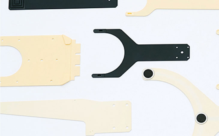
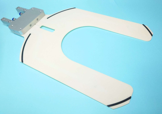
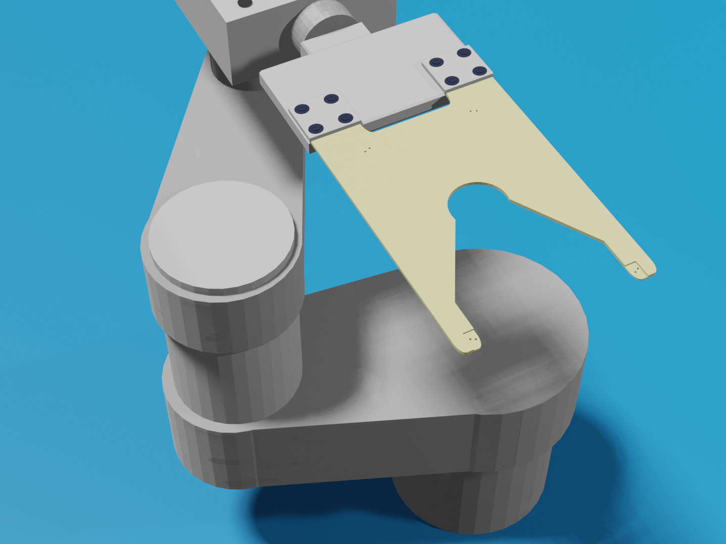
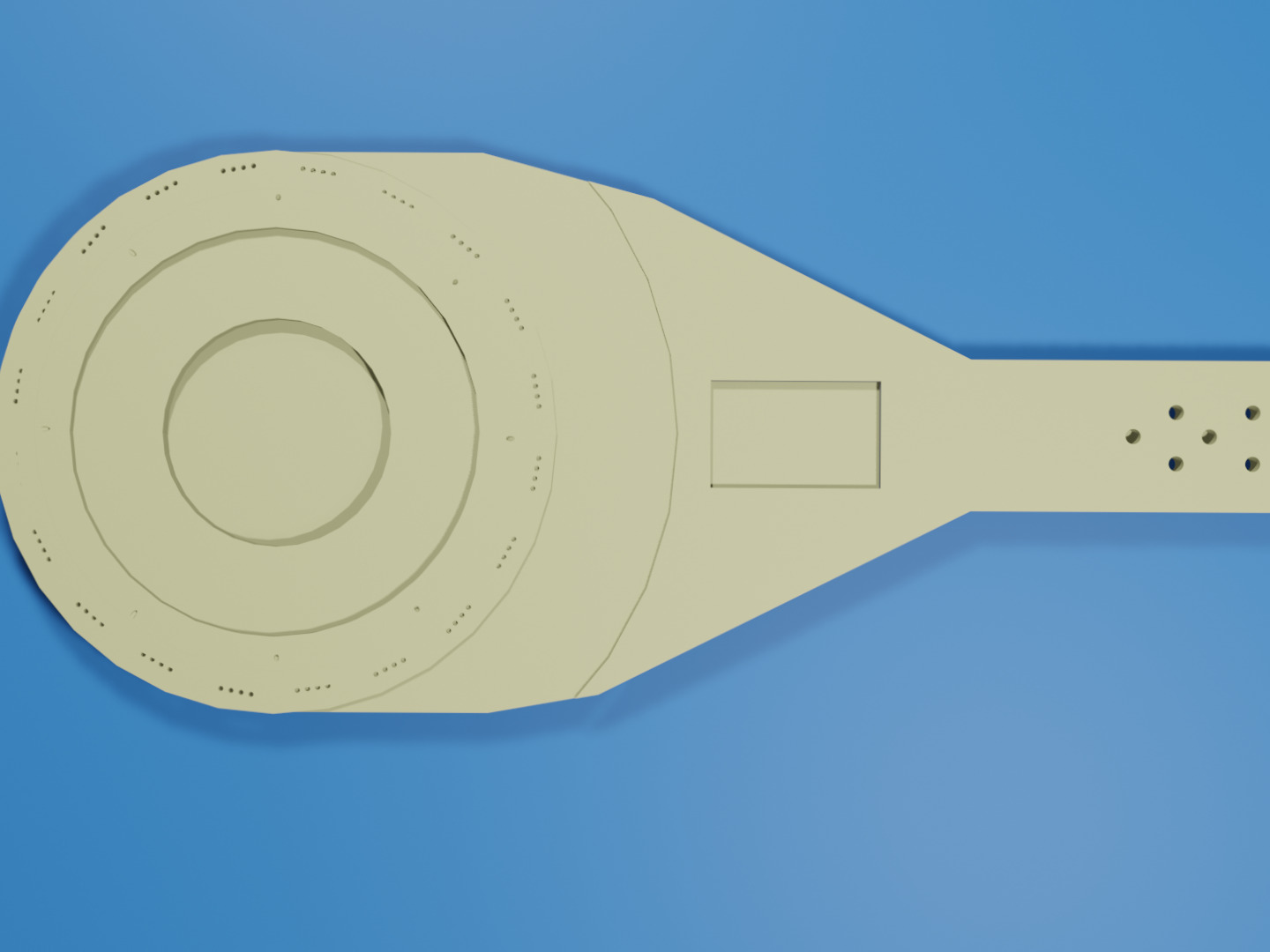
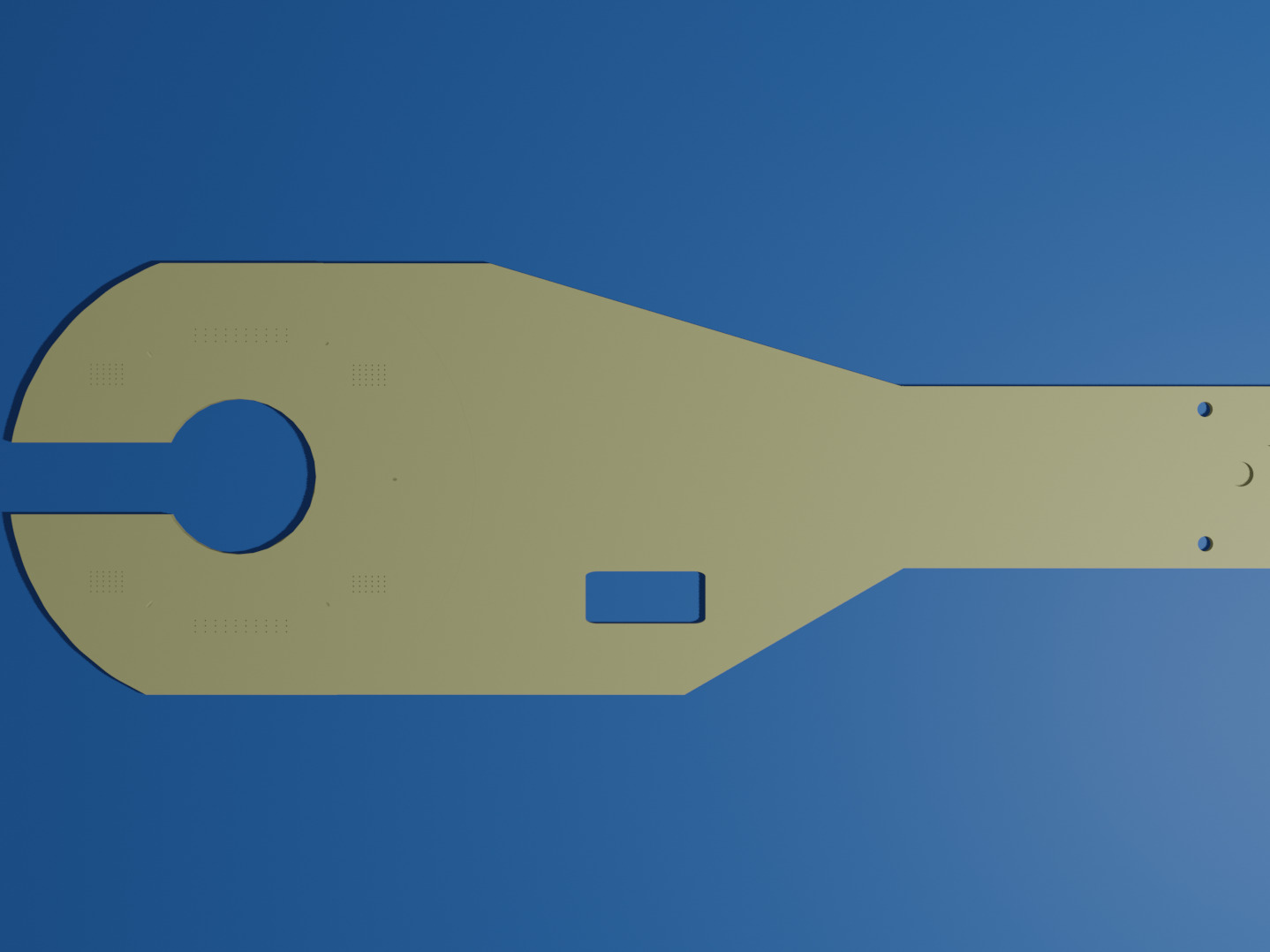
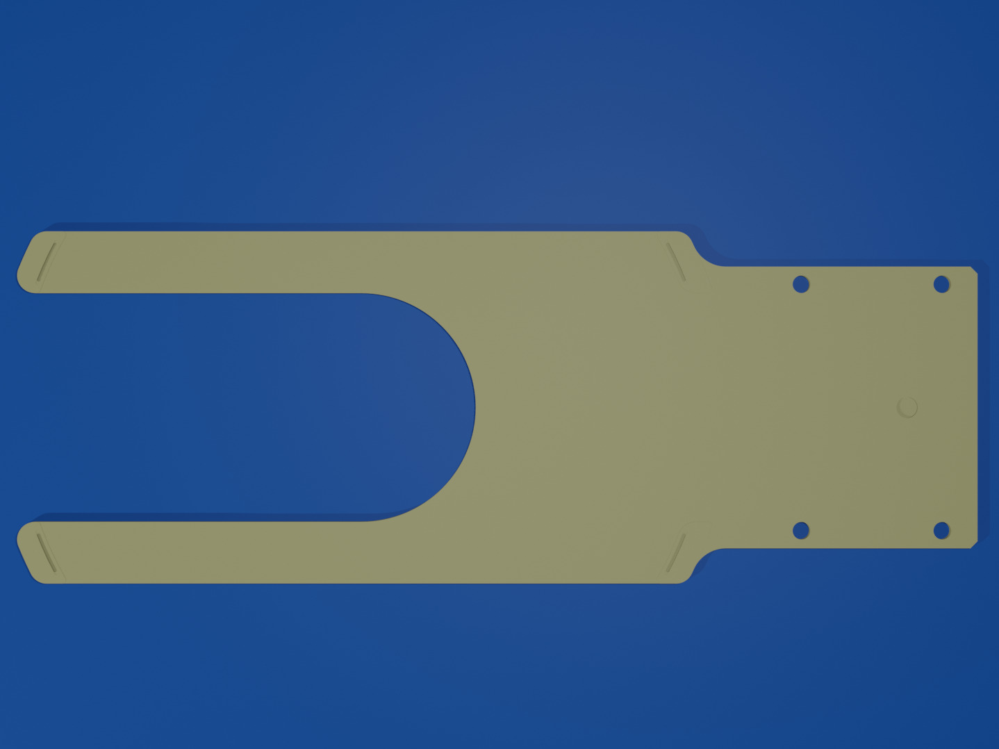
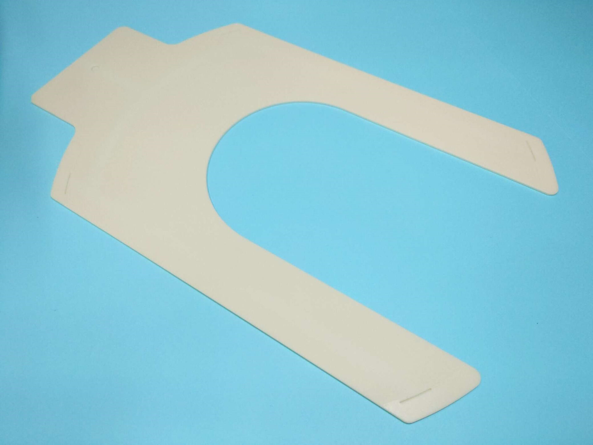
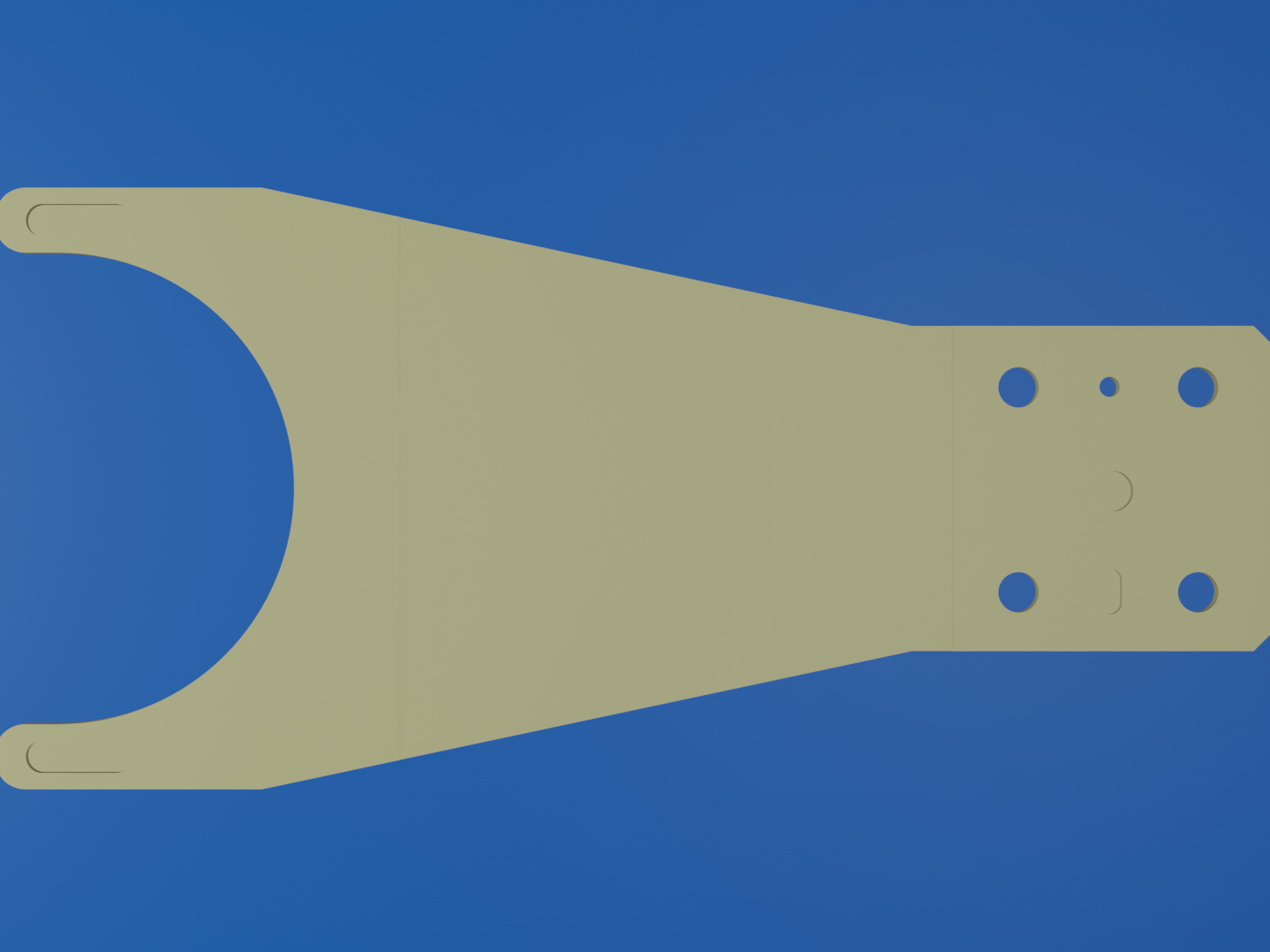
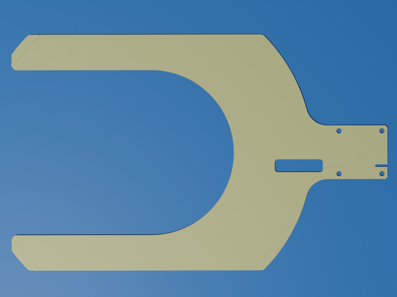
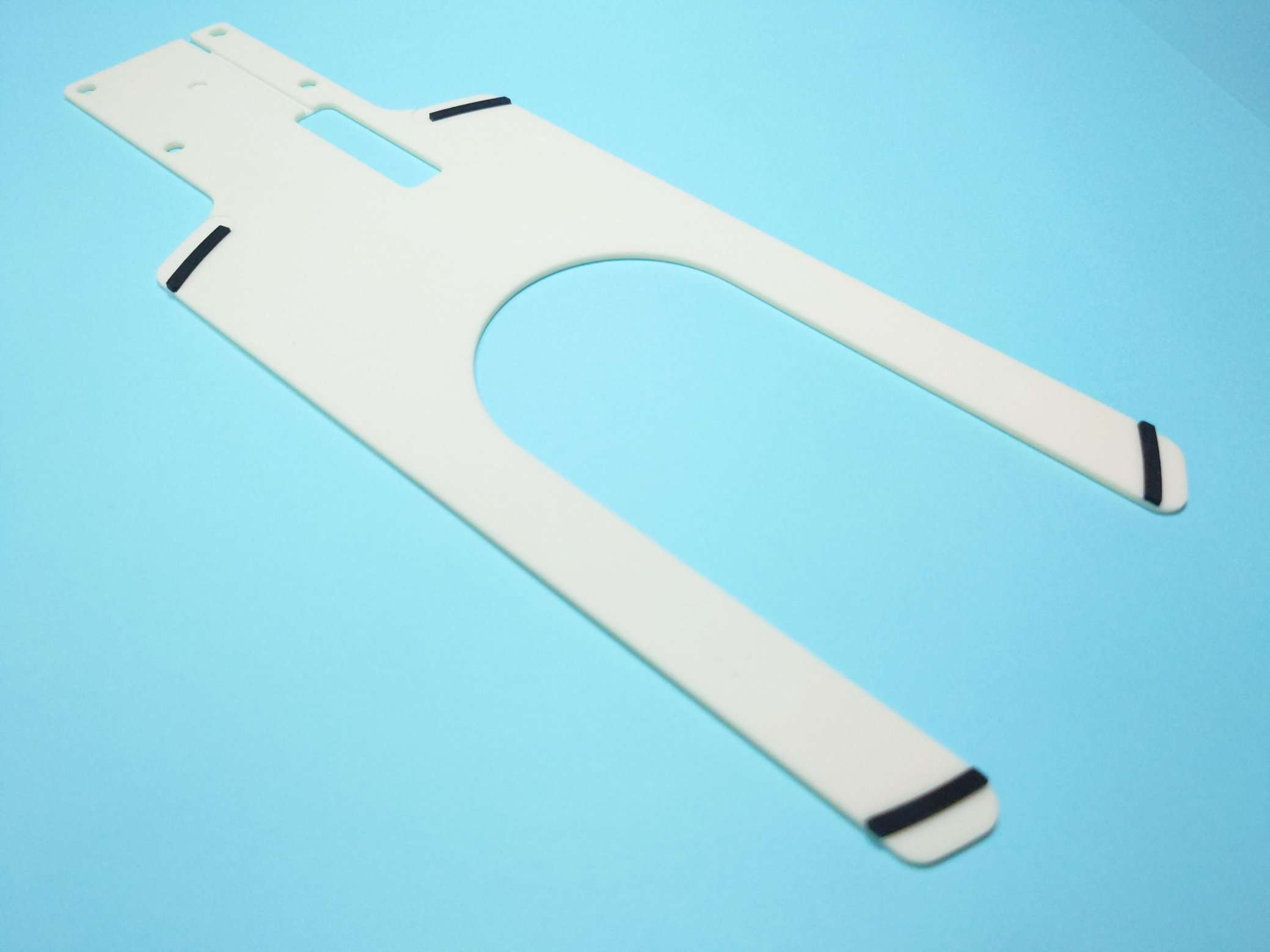
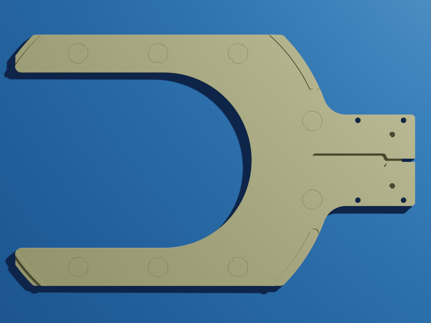
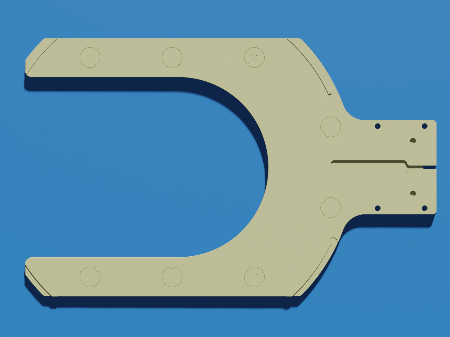
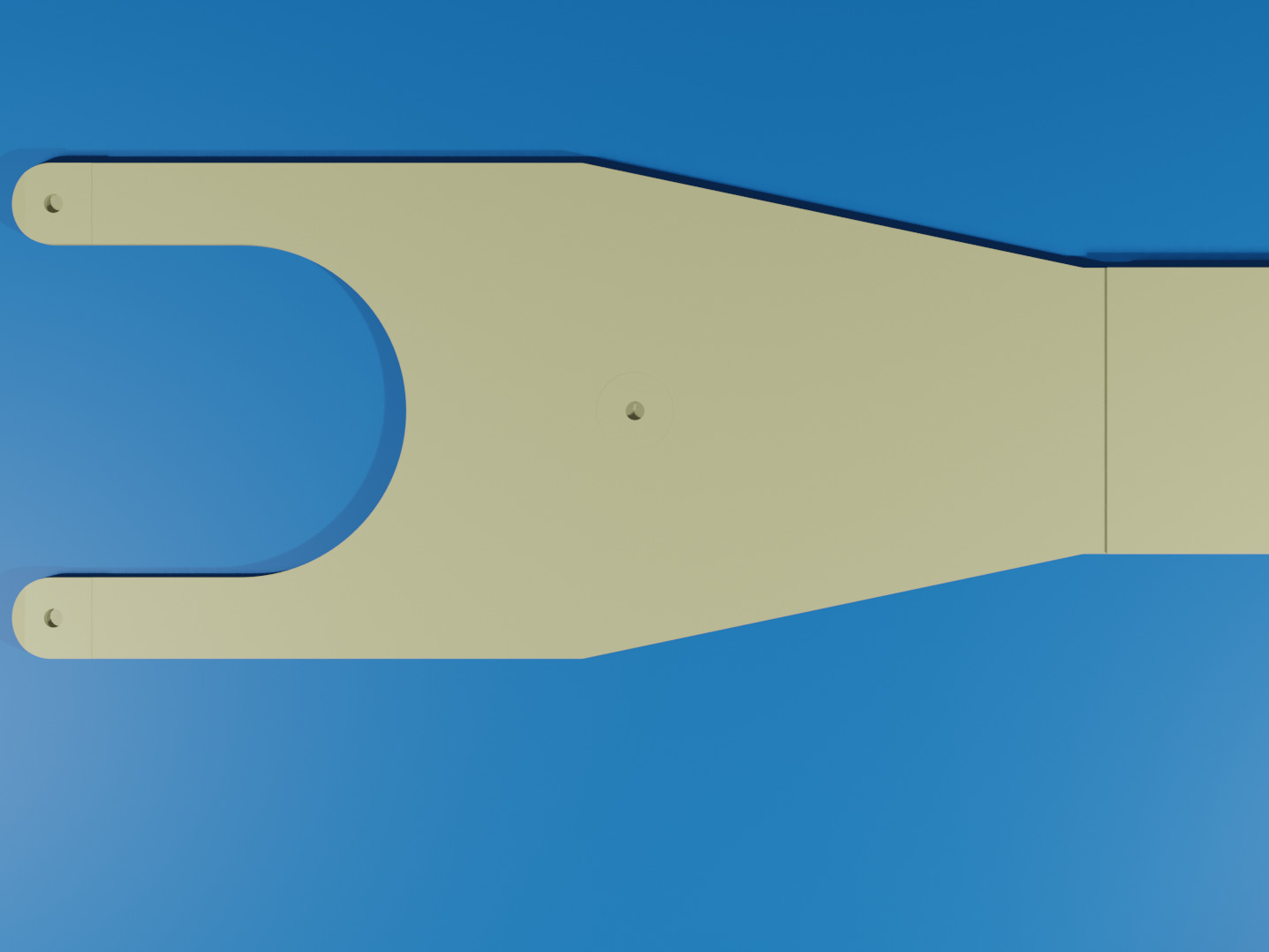
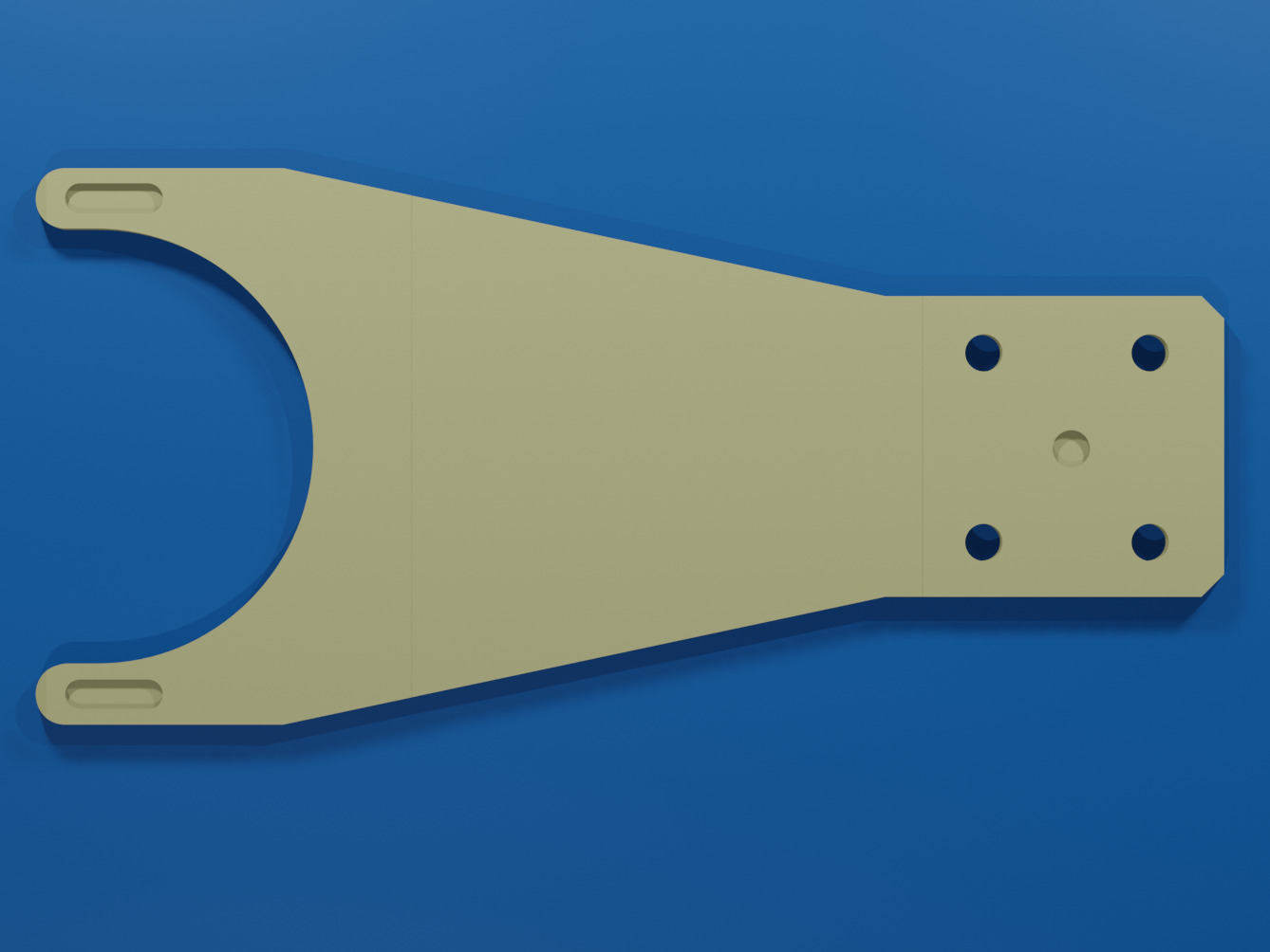
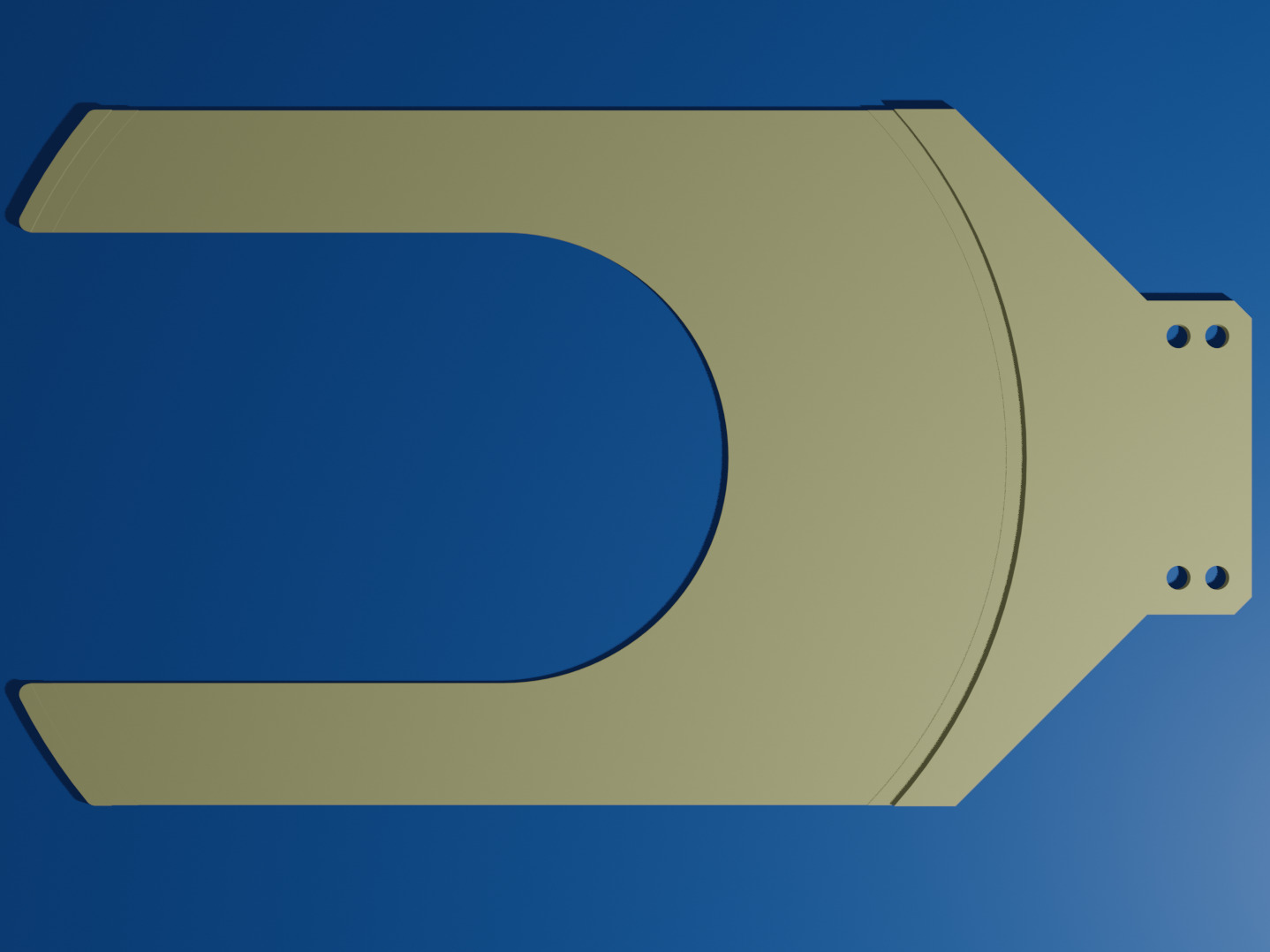
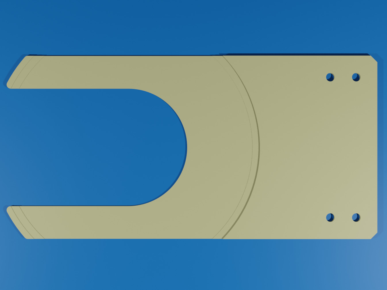
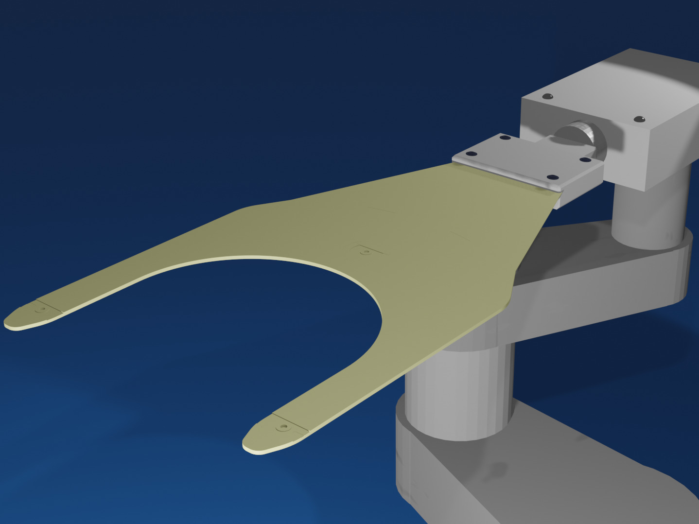
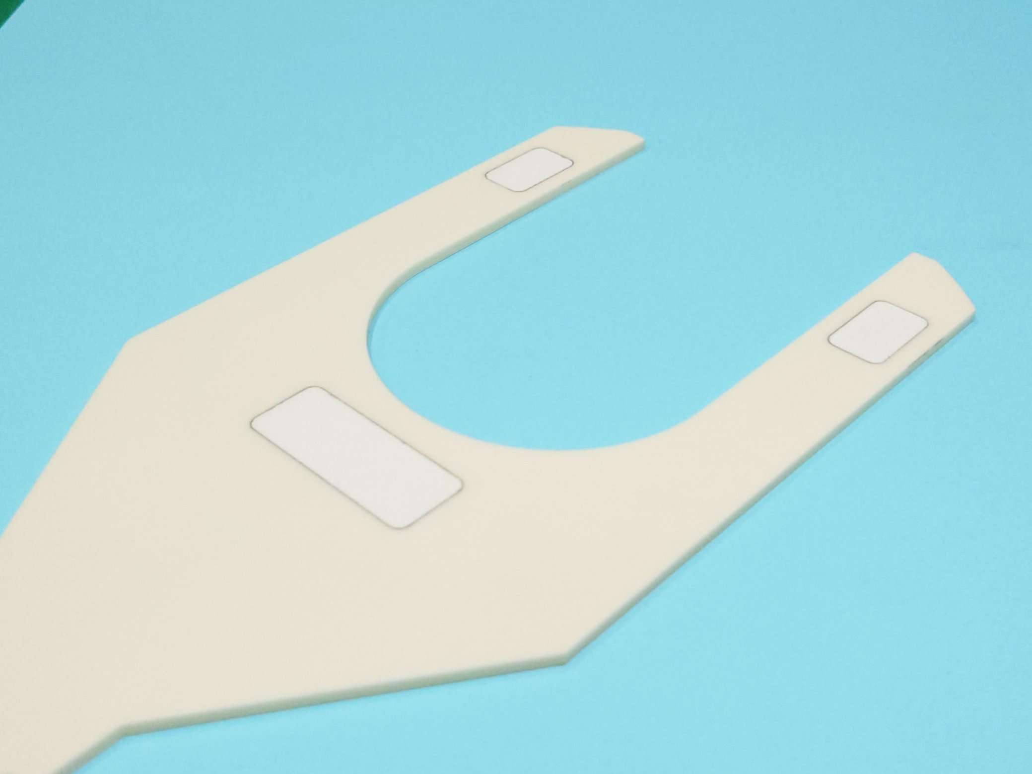
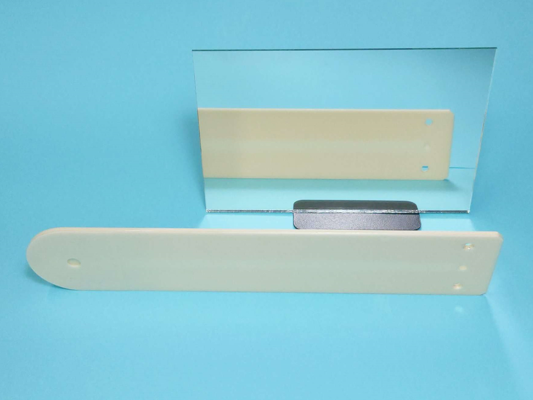
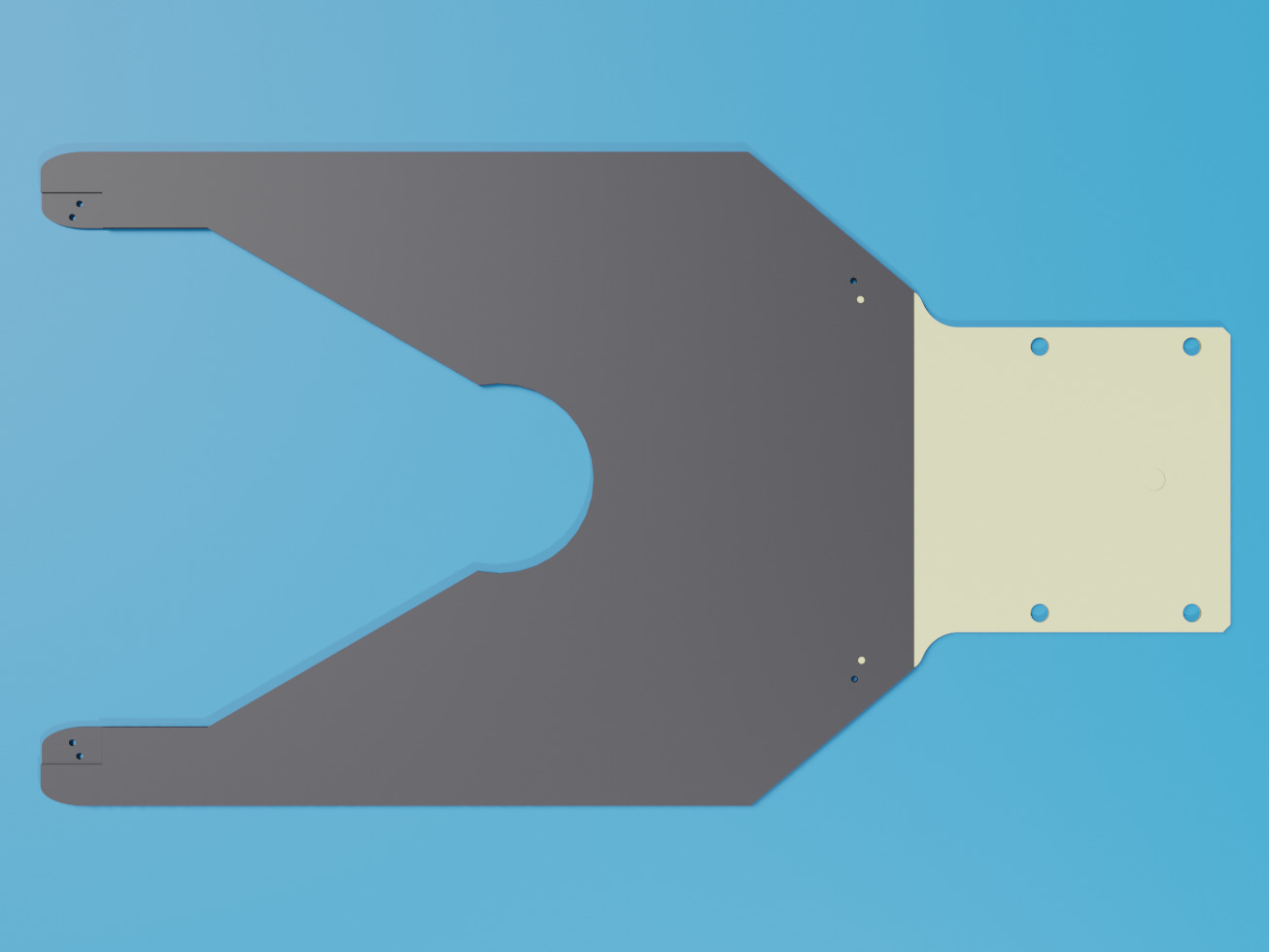
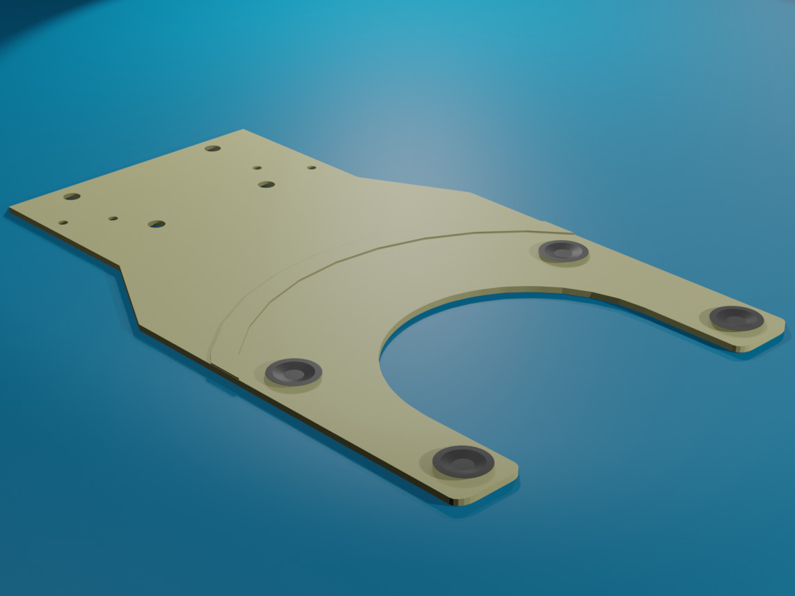
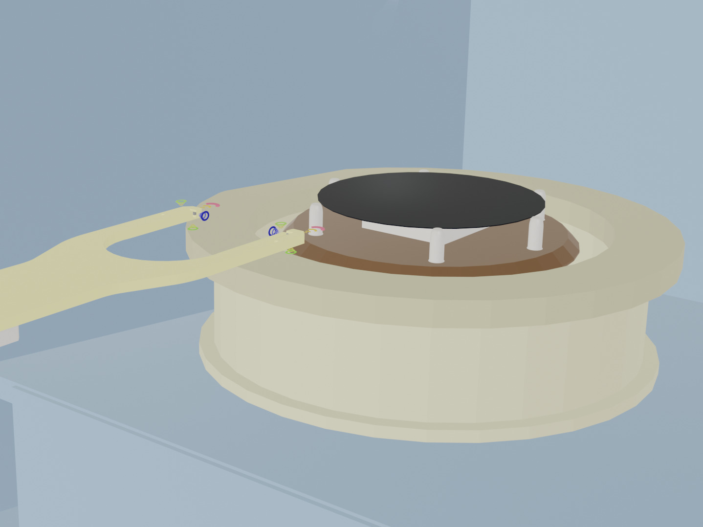
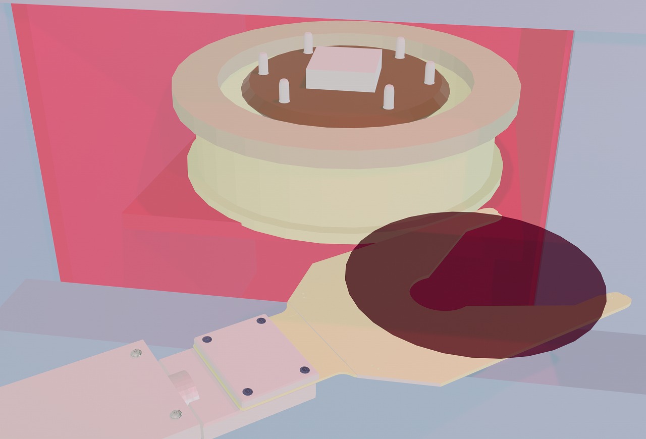
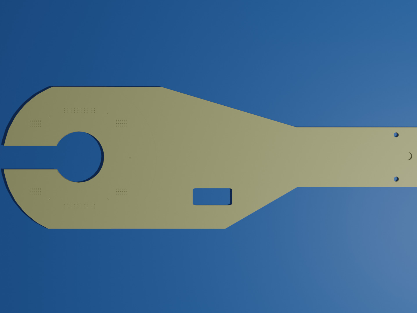
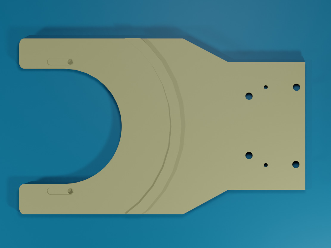
  • It is possible to rent our original the End Effector / Handling Arm demonstration machine. Ejectors for suction End Effector / Handling Arm are available. The equipment can be used immediately as long as compressed air is available. If you need a wrist block or other parts for installation of the device, we can make them for you. We have a lineup available for loan, so please contact us for details.

  • Yes, it is possible. Usually, sensors are installed in the groove. As a special example, a sensor that crawls on the side of the transfer End Effector / Handling Arm or a type that passes the sensor inside the cavity is available. Please feel free to contact us if you have any requests such as wishing to attach a sensor or arranging a transfer End Effector / Handling Arm with a sensor.

  • Yes, it is possible. As an example of improvement, some customers attach metal arms to their End Effector / Handling Arm and use them to transport and unload wafers.


    >>Details are here.

Four Reasons Why Ceramics Design Lab is Chosen

  • Integrated support from material development to design and manufacturing of ceramics

    Integrated support from material development to design and manufacturing of ceramics

    We produce a wide variety of fine ceramics products such as Alumina, silicon carbide (SiC), Zirconia, Porous ceramics, etc.We are familiar with the types and characteristics of fine ceramics materials, as well as the usage environment and applications of products used in semiconductors, electronic components, and other fields, enabling us to make optimal material proposals.Our in-house facilities and equipment for mixing and granulating raw materials, as well as for forming materials, enable us to develop special materials such as insulating ceramics, conductive ceramics, low-reflective Black Alumina, and high-purity ceramics, so that we are able to contribute to the solution of our customers’ issues.
  • Extensive delivery record for semiconductor foundries, electronic device manufacturers, and equipment manufacturers

    Extensive delivery record for semiconductor foundries, electronic device manufacturers, and equipment manufacturers

    We have delivered ceramics products to domestic and overseas semiconductor foundries, electronic device manufacturers, and equipment manufacturers for many years.We have a proven track record in the design and manufacture of ceramic products of various shapes, applications, and materials, such as transfer End Effector / Handling Arm and suction chucks for thin work pieces such as silicon wafers and films, as well as shield parts for wafer trays, printed circuit boards, and vacuum chambers.
  • Expertise in VA / VE proposals backed by over 40 years of history

    Expertise in VA / VE proposals backed by over 40 years of history

    In the manufacturing and transport processes of semiconductors and electronic components, these problems can occur
    ・Particle generation
    ・Reduction of yield due to contamination
    ・Wafer surface damage due to misalignment
    ・Outgas (outgassing)

    We are well aware of these industry-specific problems and the reasons behind them, and is actively proposing VA・VE techniques to solve each customer’s problem.
    We can respond to customer needs by reducing costs, shortening lead times, reducing man-hours for parts replacement, and improving the functionality of the transport End Effector and Handling Arm.
  • Consignment services from prototyping to mass production of one-off products

    Consignment services from prototyping to mass production of one-off products

    We specialize in small-lot, high-mix production, and can flexibly handle everything from trial production of single and small lots to mass production of medium lots of up to about 100 pieces.

    During prototyping, we make material and design proposals that take into account the product application and operating environment according to the customer’s requirements. We evaluate mass production feasibility such as cost, lead time, and accuracy variation before moving to mass production, so there is no rework.

Operating company information

Company Name ASUZAC CORPORATION
Division name Fine Ceramics Division
Division established October, 1981
Address Headquarters: 981 Oaza Nakayama, Takayama-mura, Kamitakai-gun, Nagano 382-8508, Japan
factory Takayama factory
Sales Offices Headquarters, Tokyo, Osaka and Kyushu
TEL +81-26-248-1626
FAX +81-26-251-2160
Mail fcerainf@asuzac.co.jp
Description of Businesses Development, production, processing, and sales of ceramics

CONTACT

The quotation and inquiries are available by the telephone /FAX or the mail .