-
ProblemsWarped Wafer
Wafer Scratching
Misalignment -
Proposed EffectWarped Wafer Prevention
Misalignment Prevention
Improved Functionality
Yield Improvement -
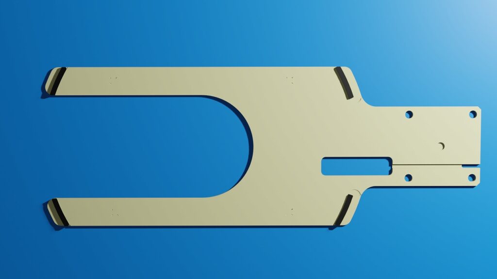
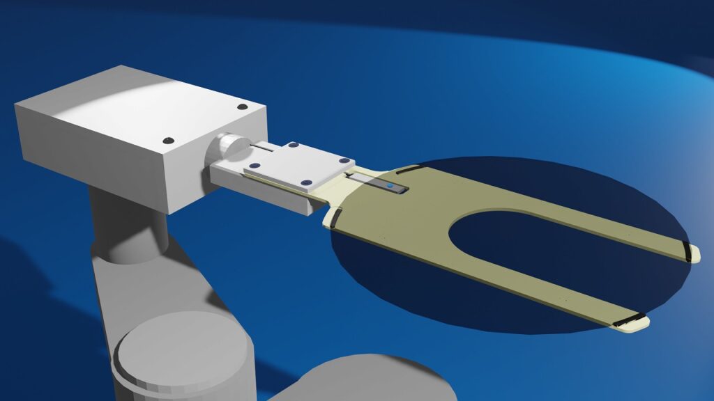
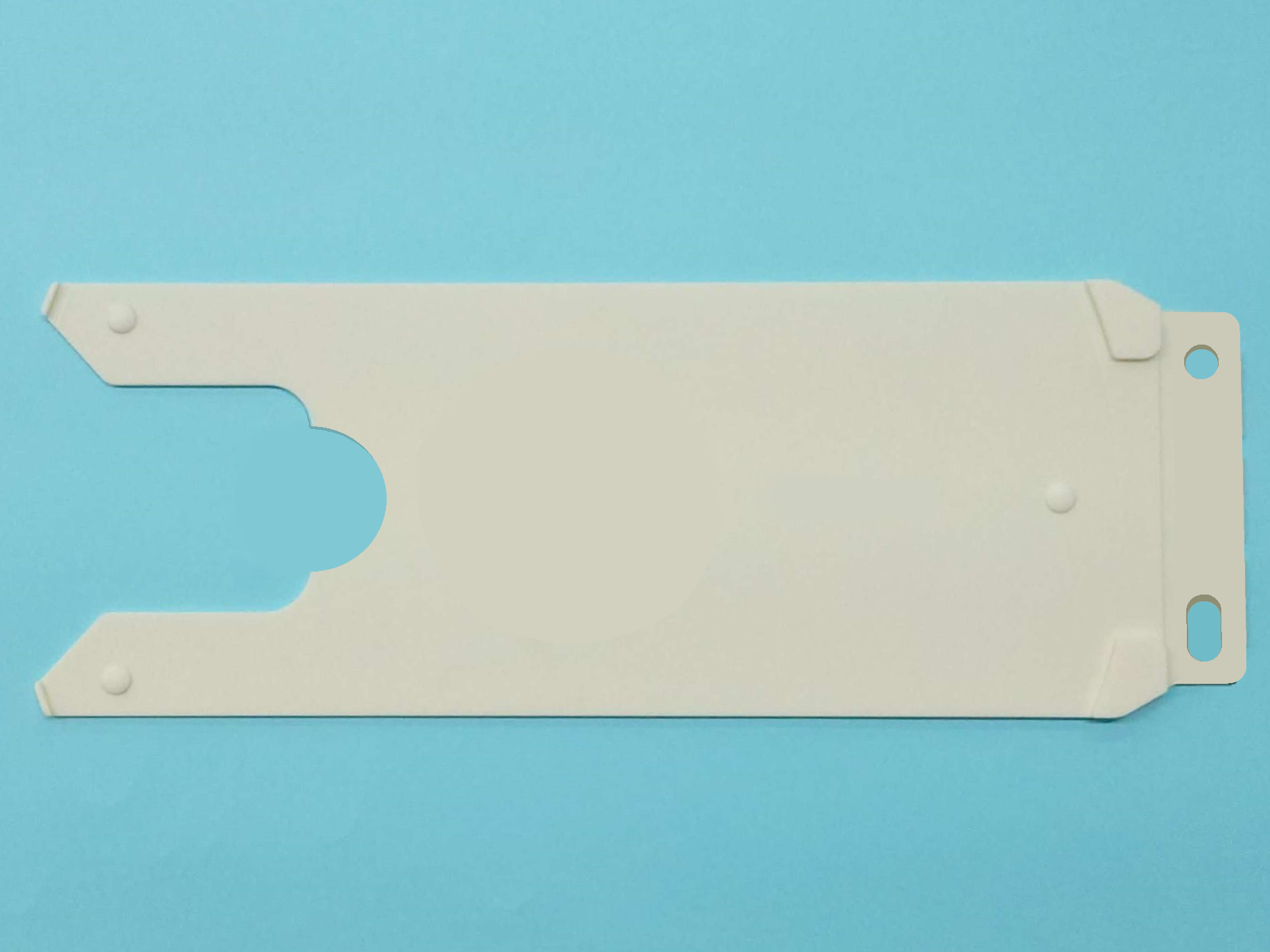
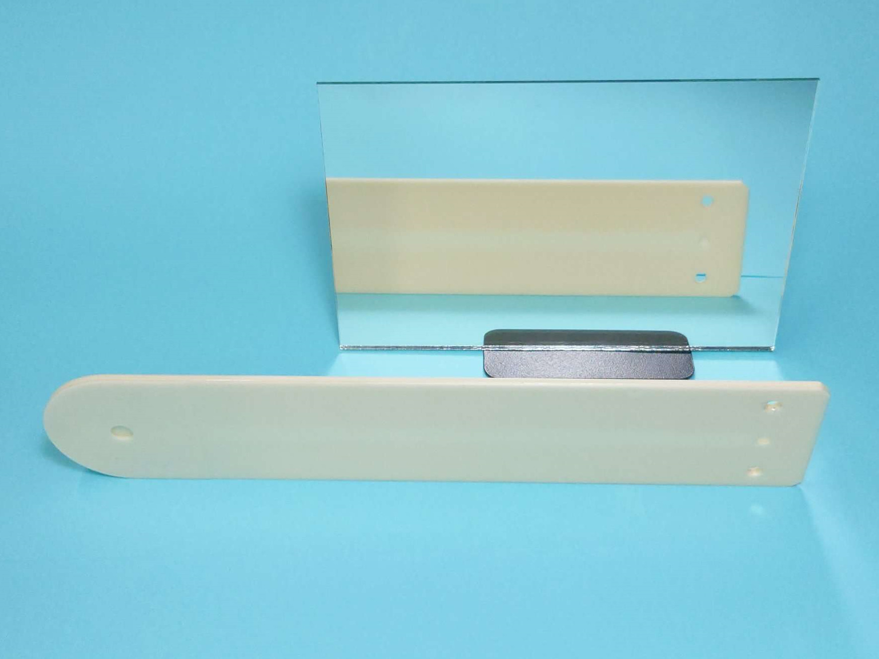
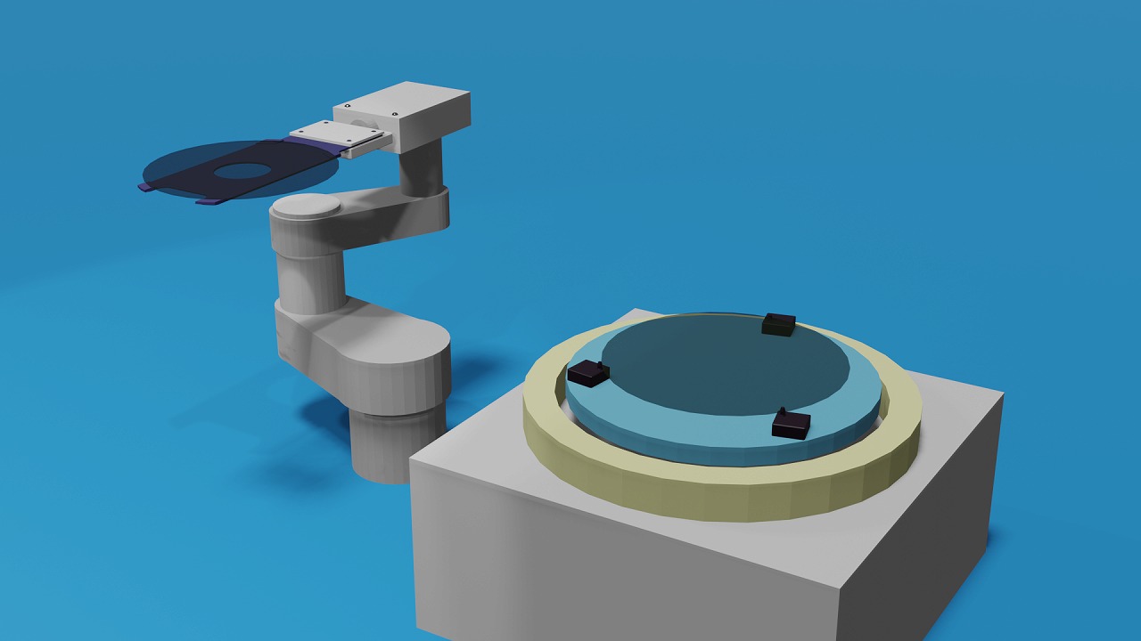
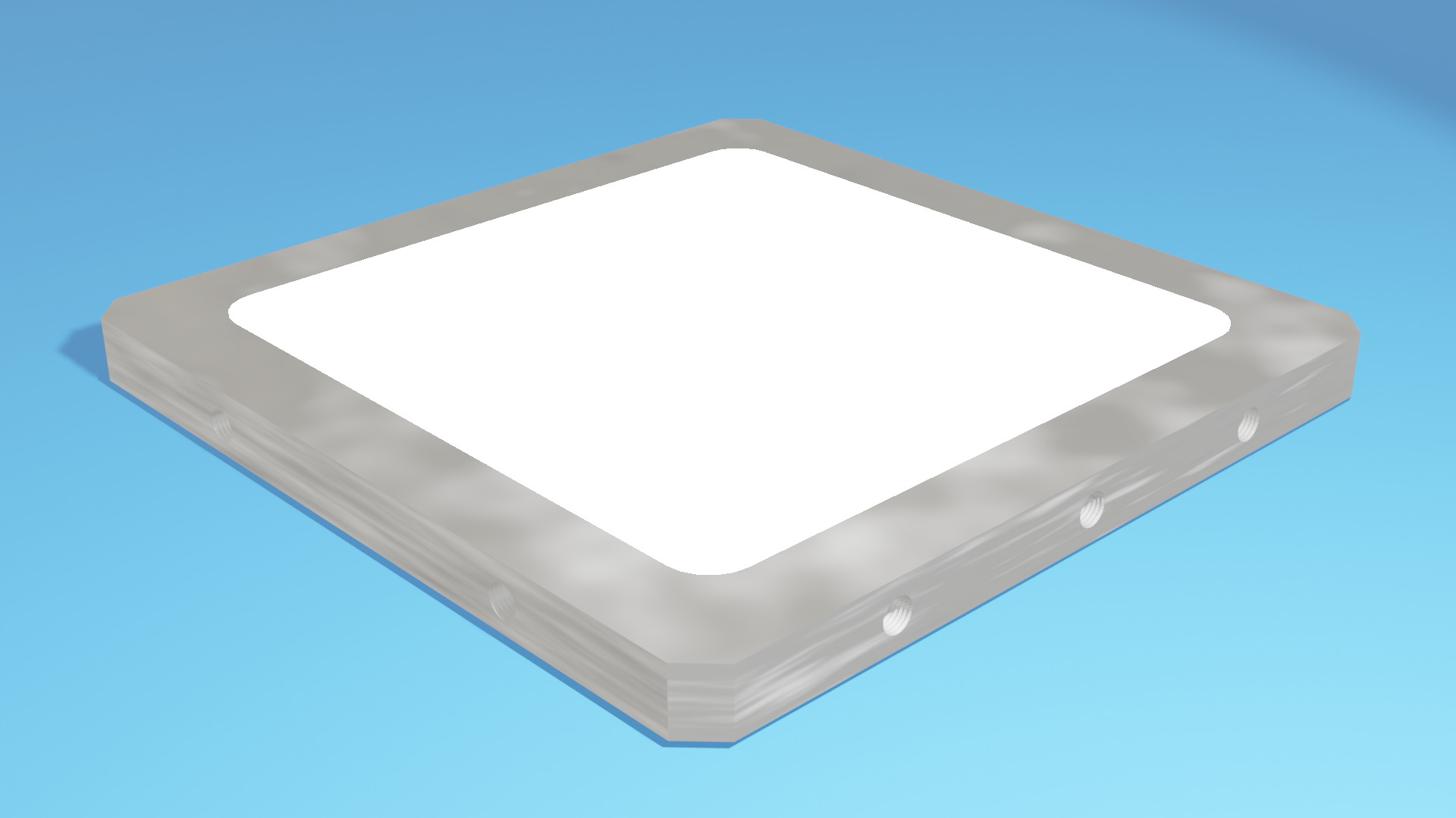
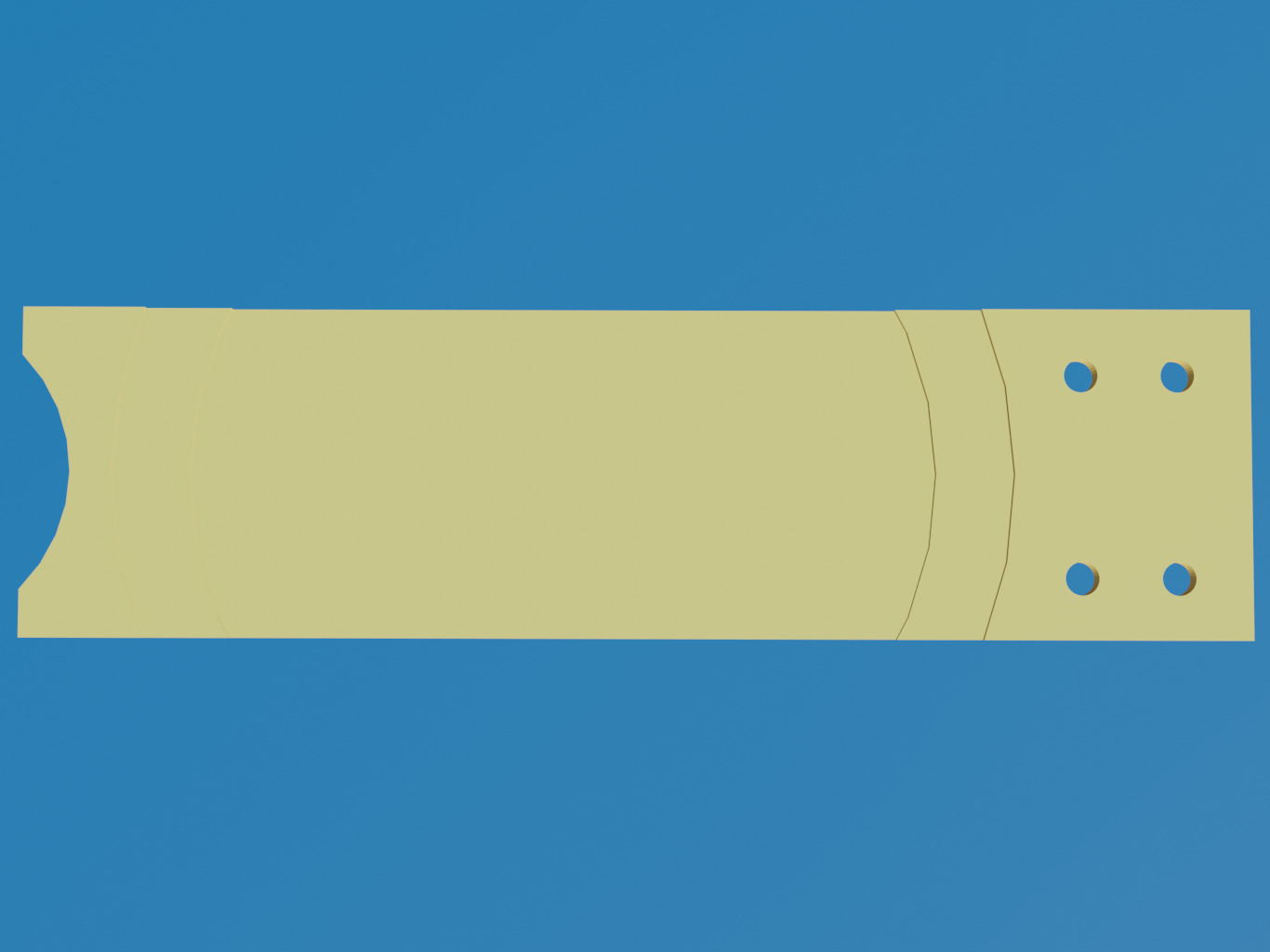
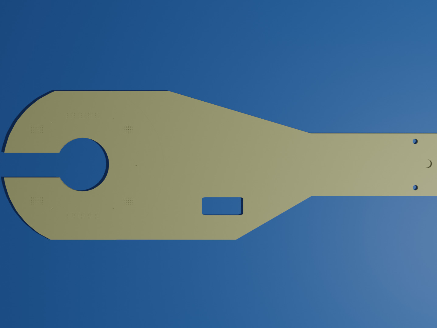
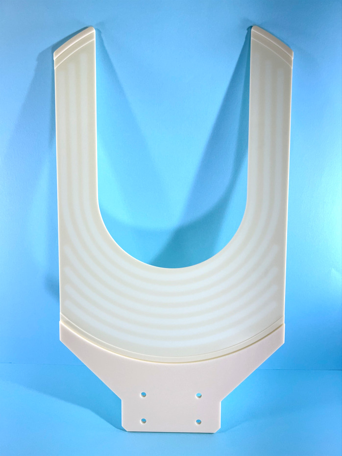
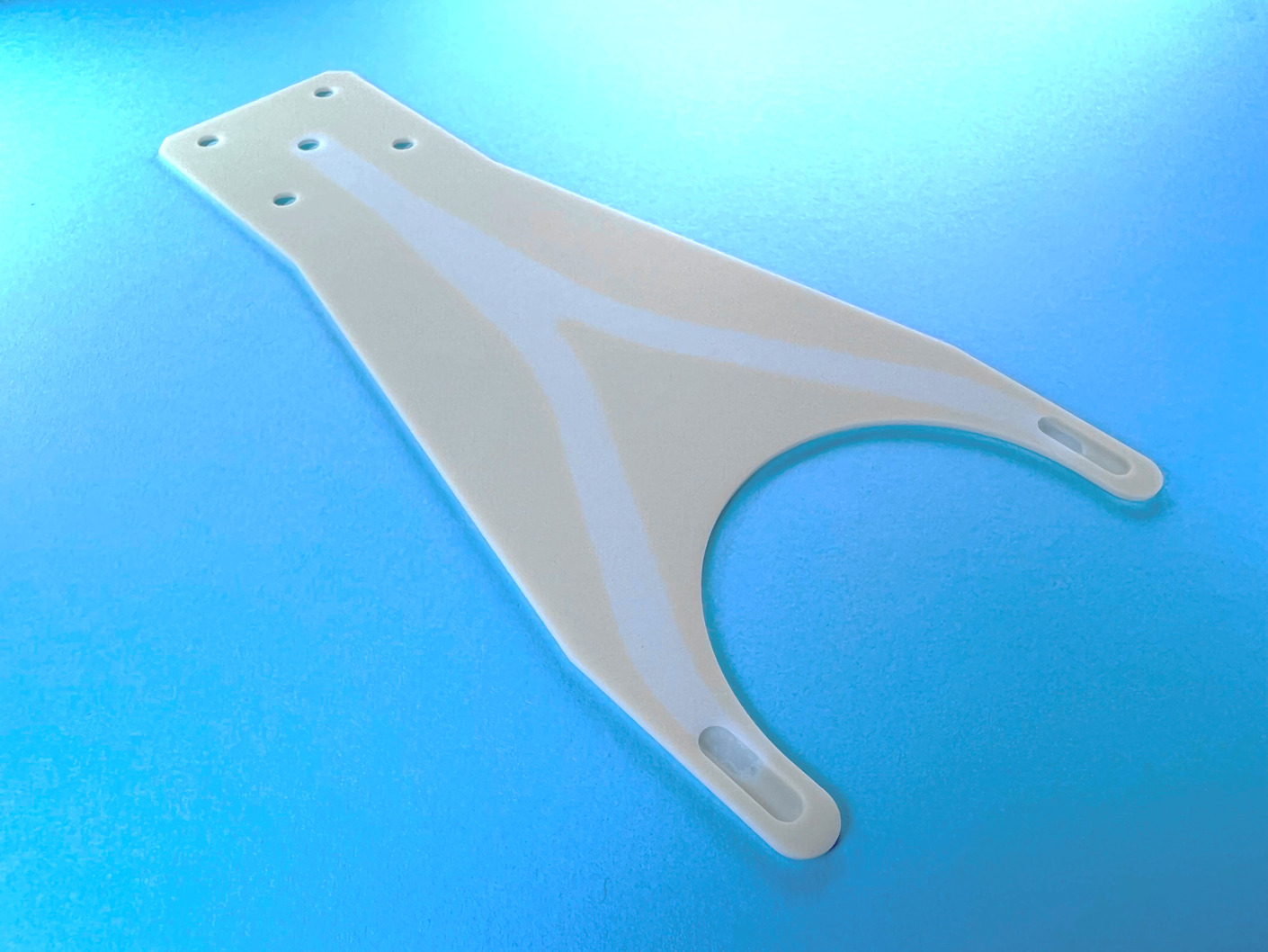
Product TypeWafer Transfer End Effector / Handling Arm
Customer's concerns and problems / Before
Our proposals and improvement effects / After
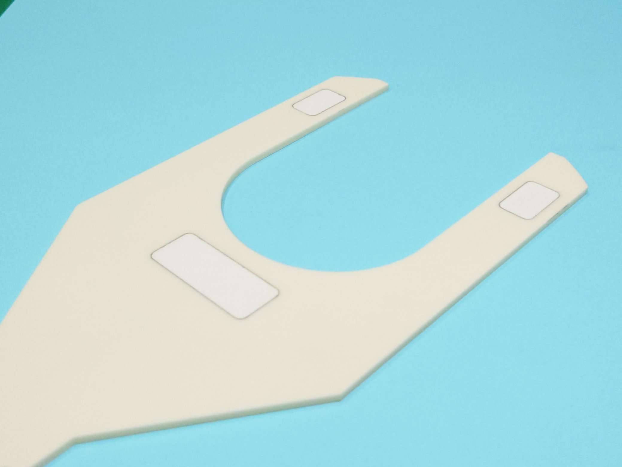
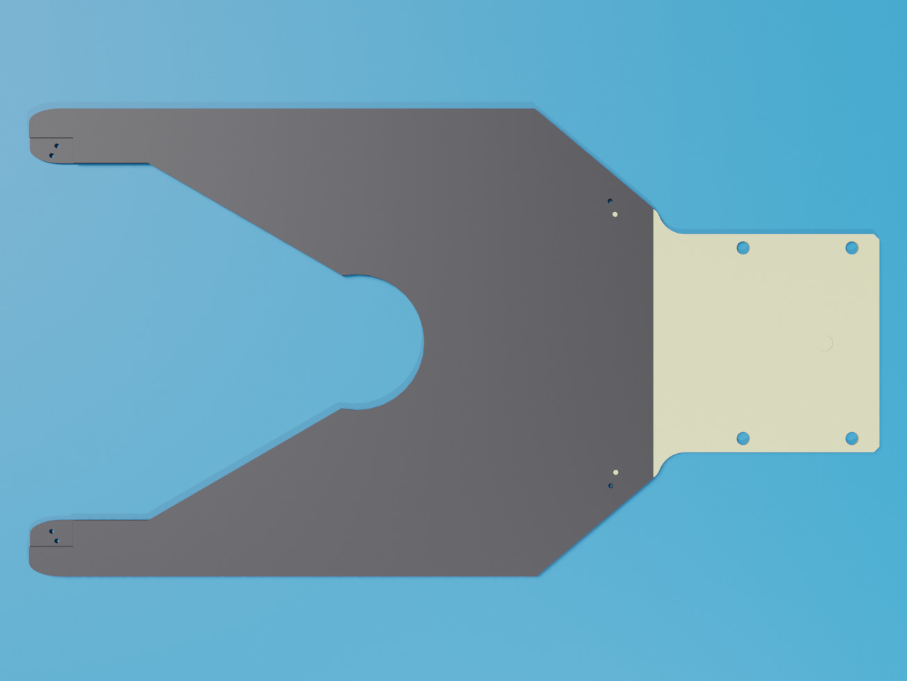
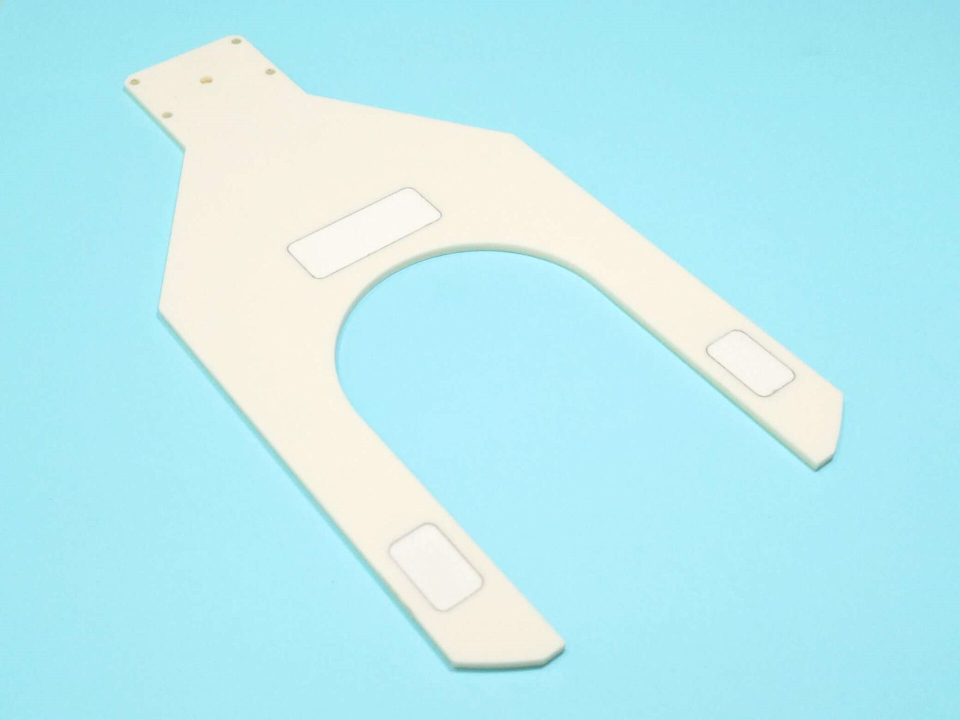
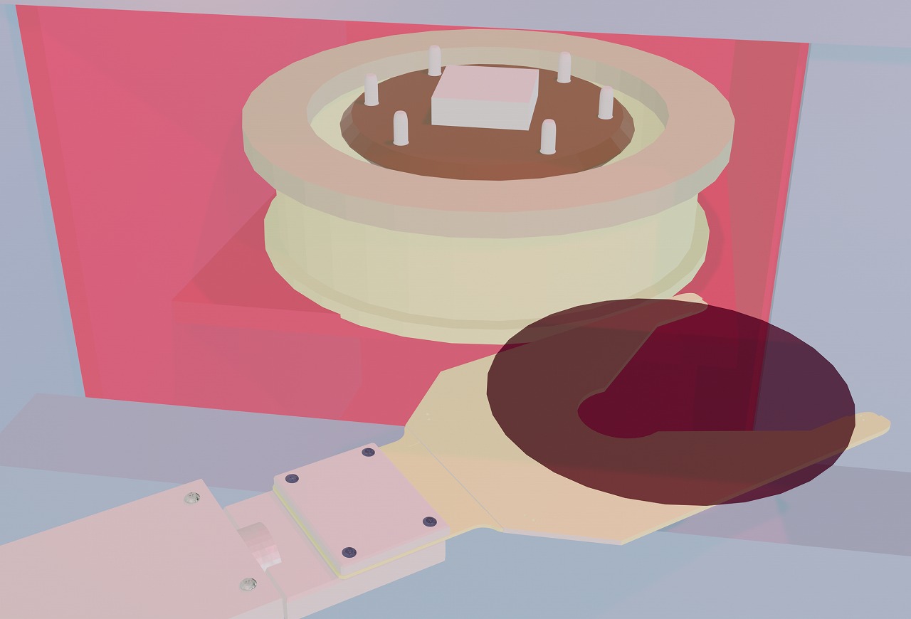
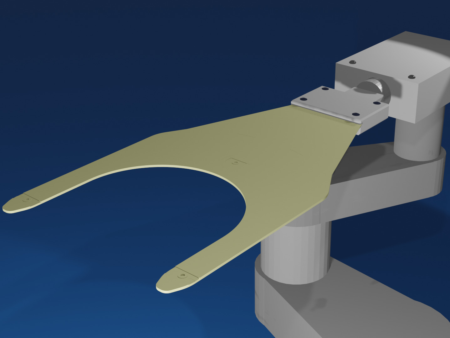
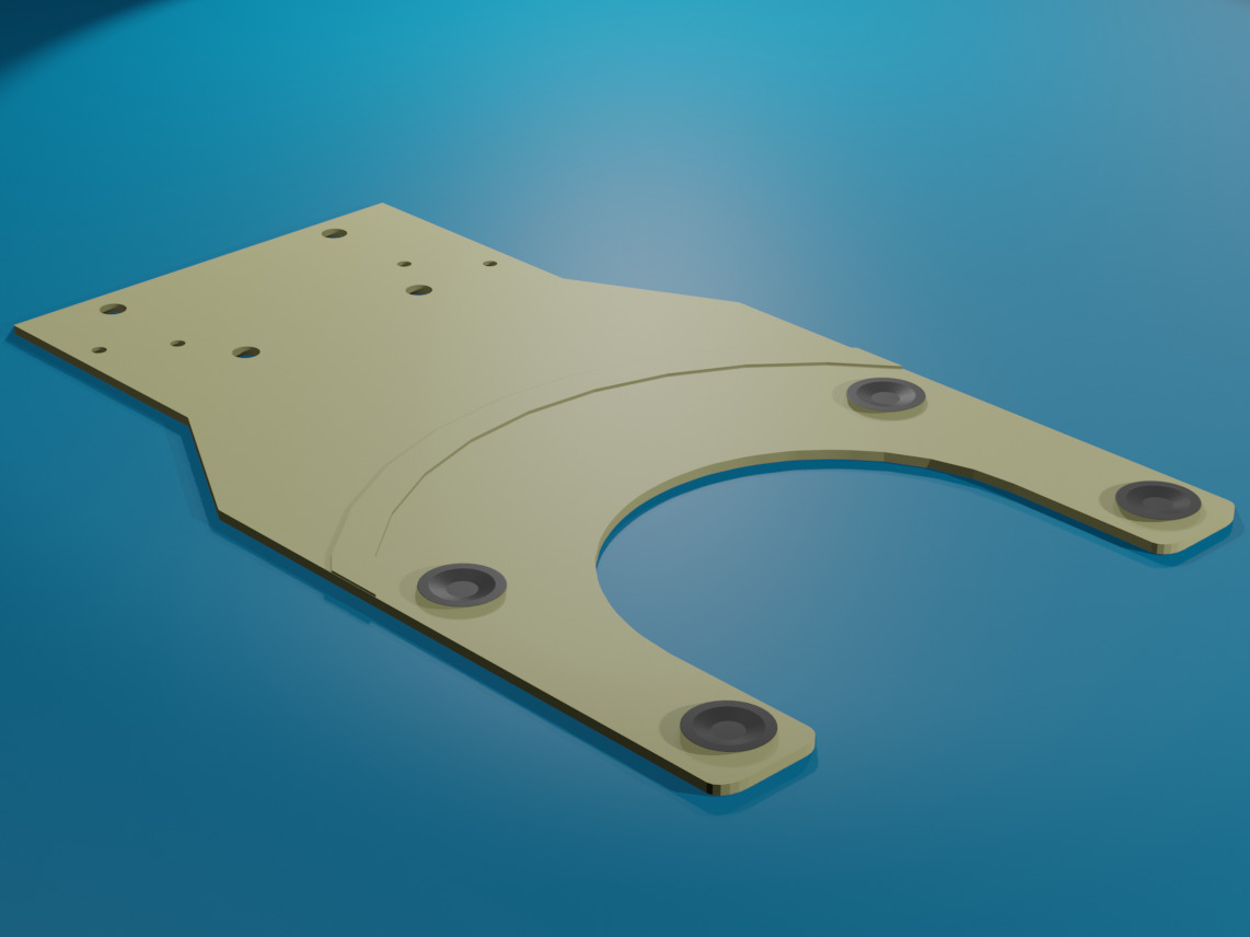
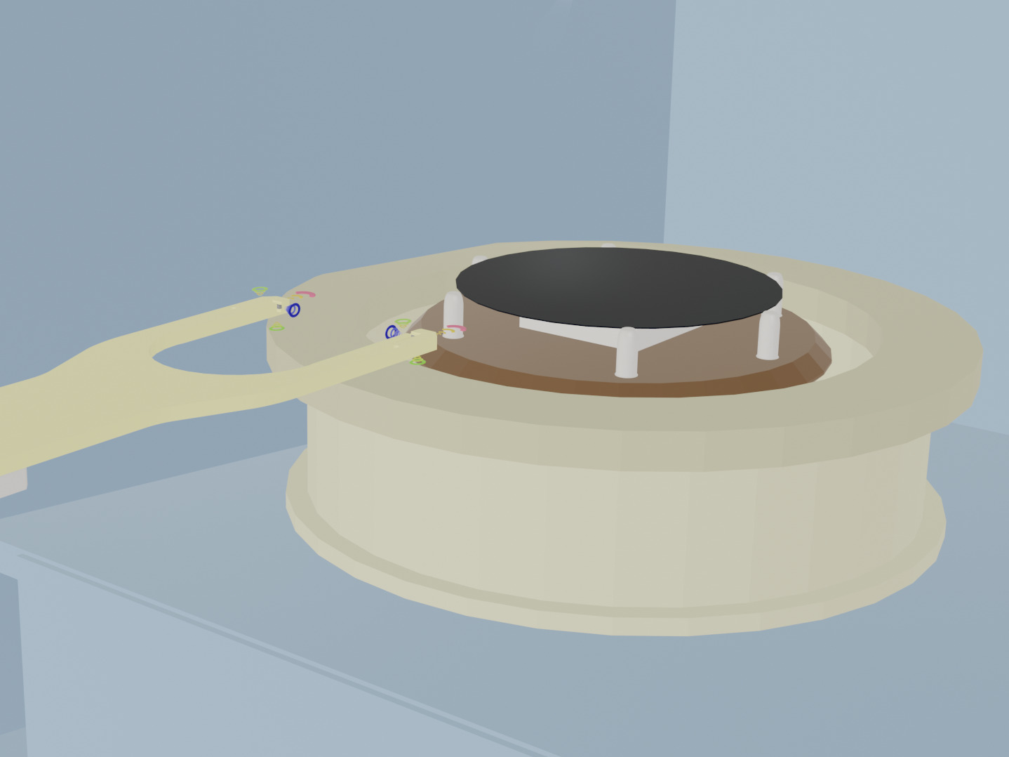
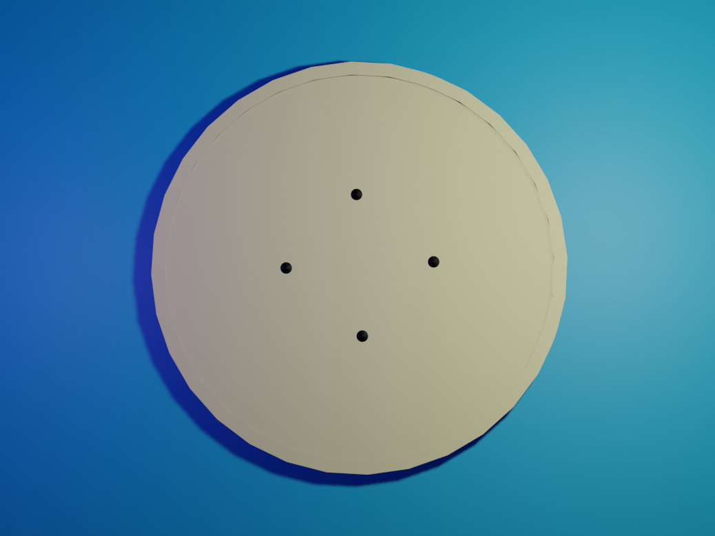
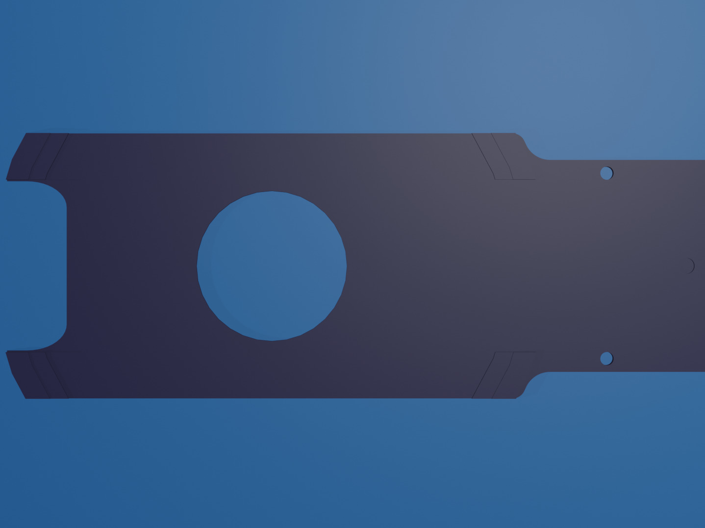
Therefore, the Ceramics Design Laboratory proposed a Transfer End Effector / Handling Arm with six suction holes on the circumference along the wafer periphery so that 6-inch warped wafers can be stably sucked.
Design and manufacture were conducted in-house, and when they were evaluated by the customer, they said that they could be used without any problems.
Point of the proposed example / Point
The point of this case is to devise the transfer hand design so that the warped wafer can be held stably.
Warping of wafers is caused by stresses generated in various manufacturing processes including polishing, but it causes wafers to fall due to insufficient suction or vacuum leakage.
When designing a transport End Effector / Handling Arm for warped wafers, it is necessary to consider these points when designing the hand.
The Fine Ceramics Division of ASUZAC Corporation, which operates the Ceramics Design Laboratory, handles everything from material development and preparation to design and manufacture, as well as surface treatment, inspection, and cleaning.
We can also offer our own coating-technology for adding functionality to ceramics materials, as well as the selection of materials such as ceramics materials with high heat resistance and conductivity, and high-purity alumina and SiC that are highly pure and prevent contamination.
If you have any questions about transporting warped wafers, please feel free to contact us.
Integrated response from processing to development of ceramic materials !
Please feel free to contact us !
Business hours: 9:00-17:00 (closed on Saturdays, Sundays and Holidays)


.jpg)


.jpg)


A customer of a semiconductor manufacturing equipment manufacturer asked us, “Wafers sometimes warp during the manufacturing process. Is it possible to manufacture a Transfer End Effector / Handling Arm that can pick up warped wafers?”
We have a wealth of experience in manufacturing wafer Transfer End Effector / Handling Arm.