(本体アルミ、多孔質AZP60)v1-1024x768.jpg)
(本体アルミ、多孔質AZP60)v2-1024x768.jpg)
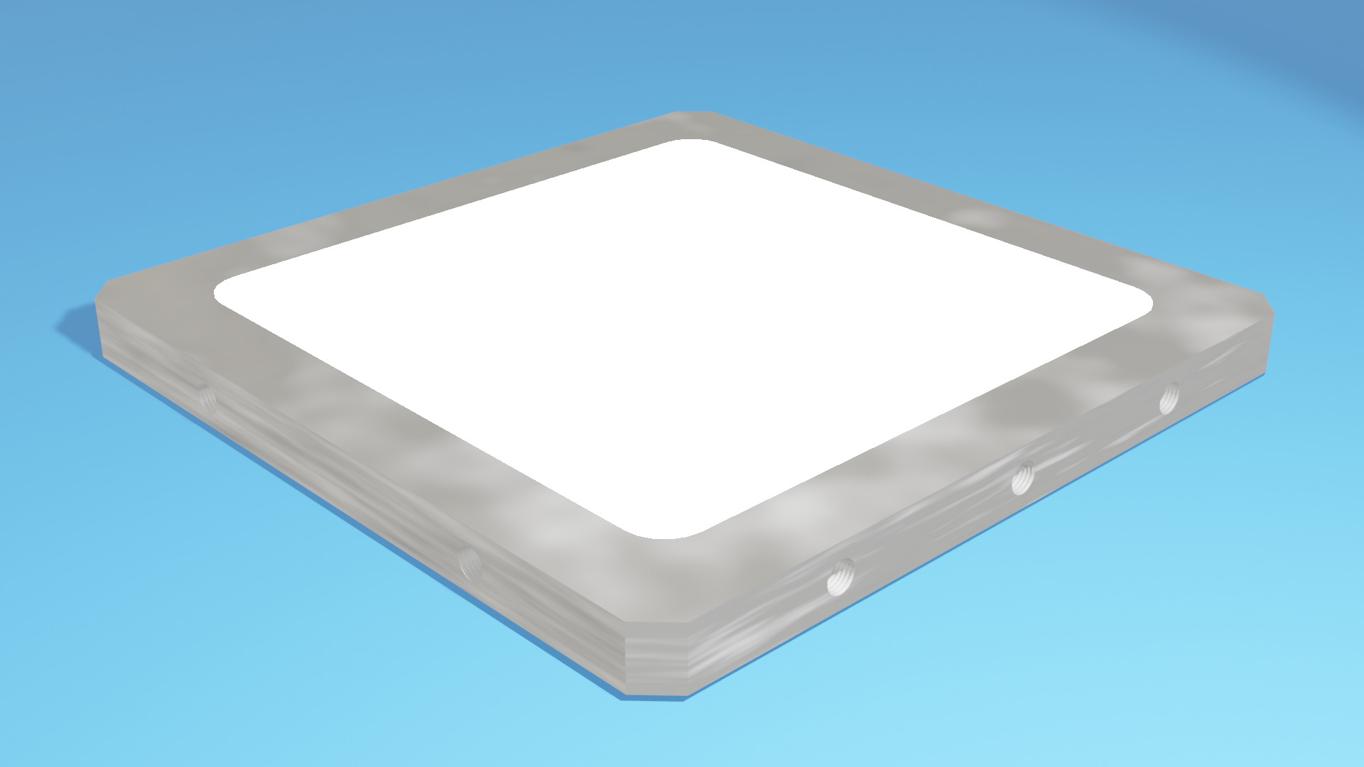
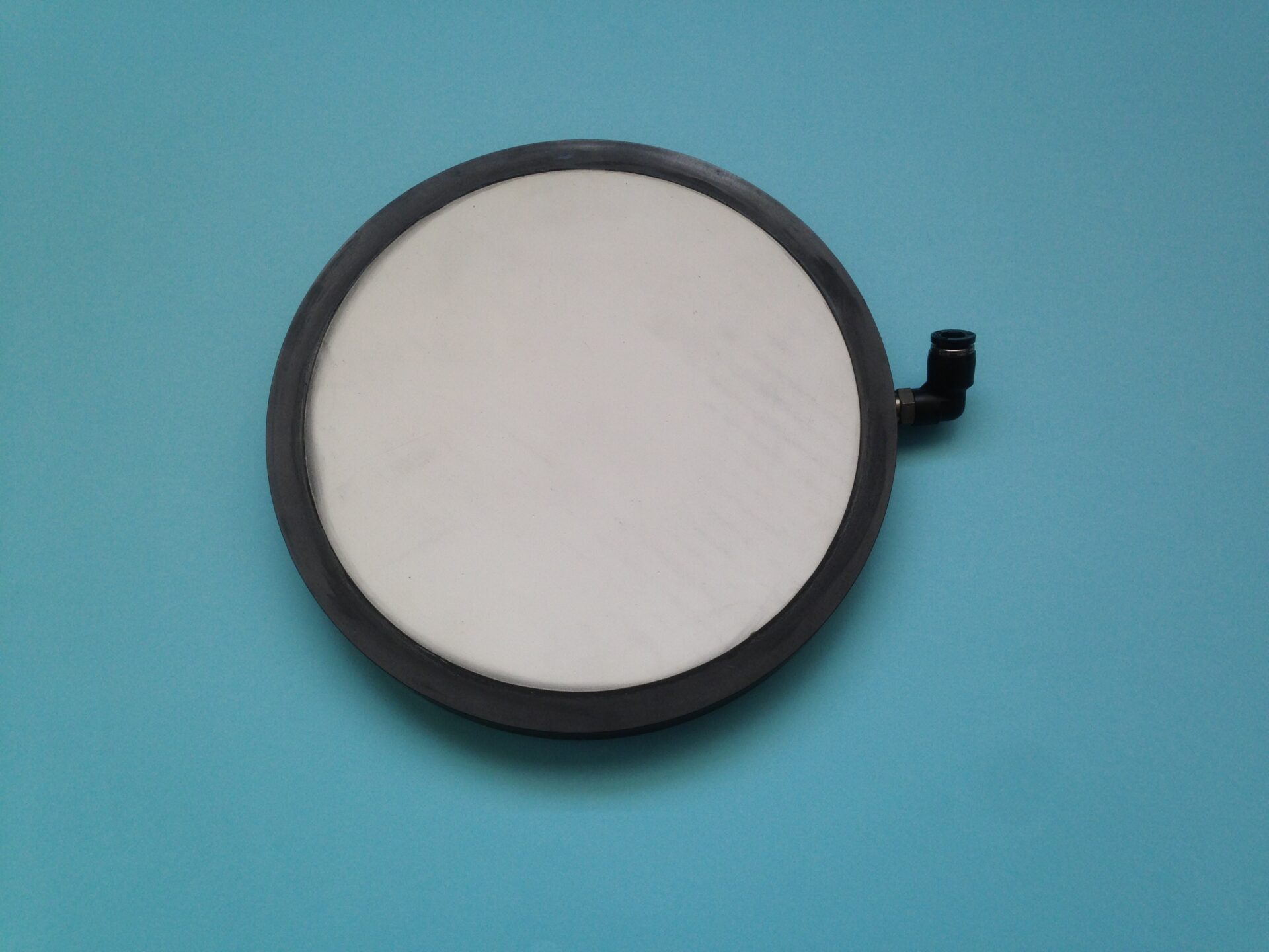
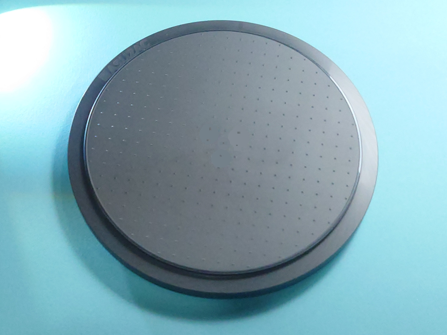
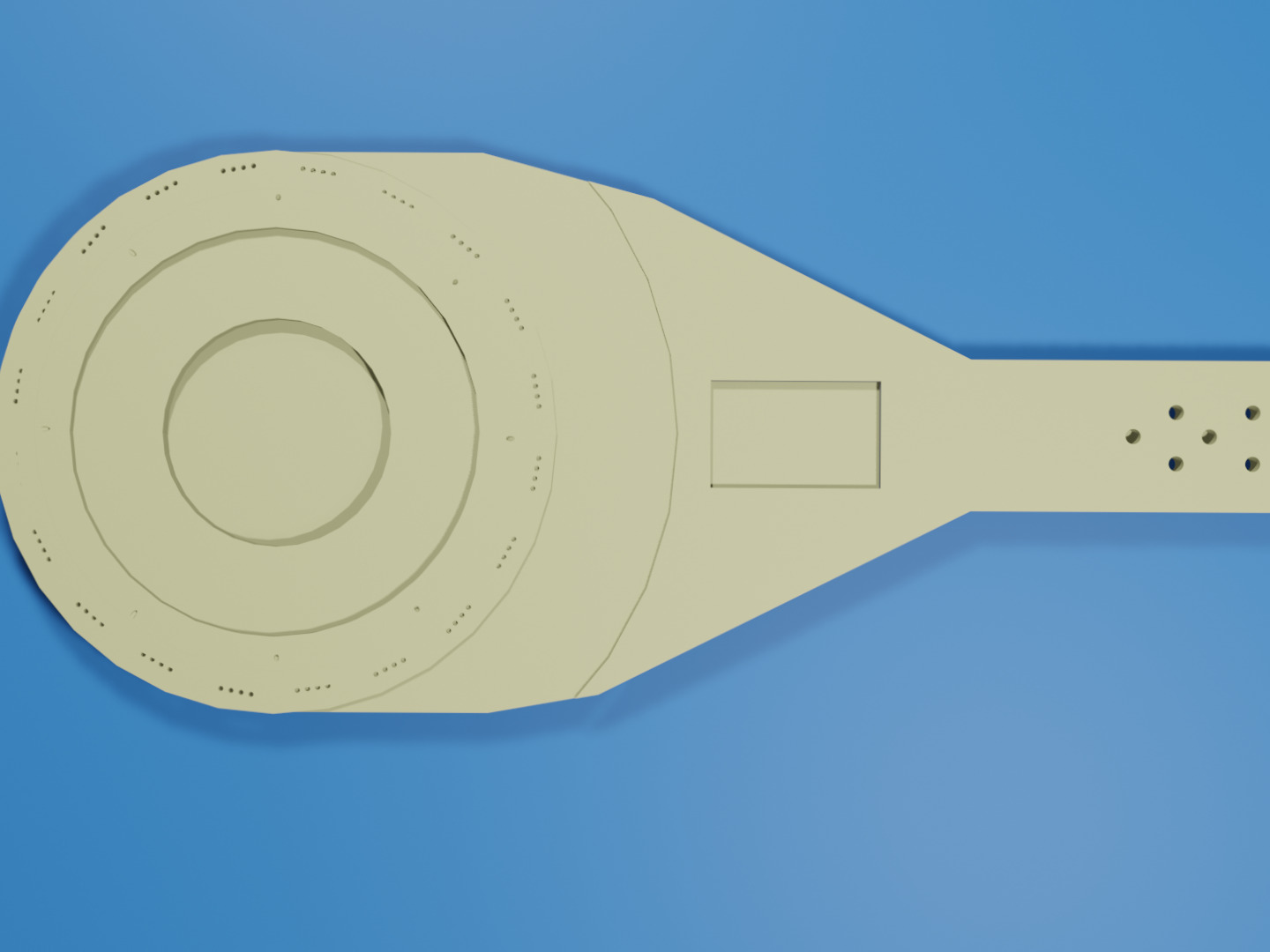
| Product Name | Porous Alumina Chuck for 6-inch wafer adsorption (Body A5052) |
|---|---|
| Industry |
Semiconductor Industrial machinery Film |
| Product Type | Porous Chuck |
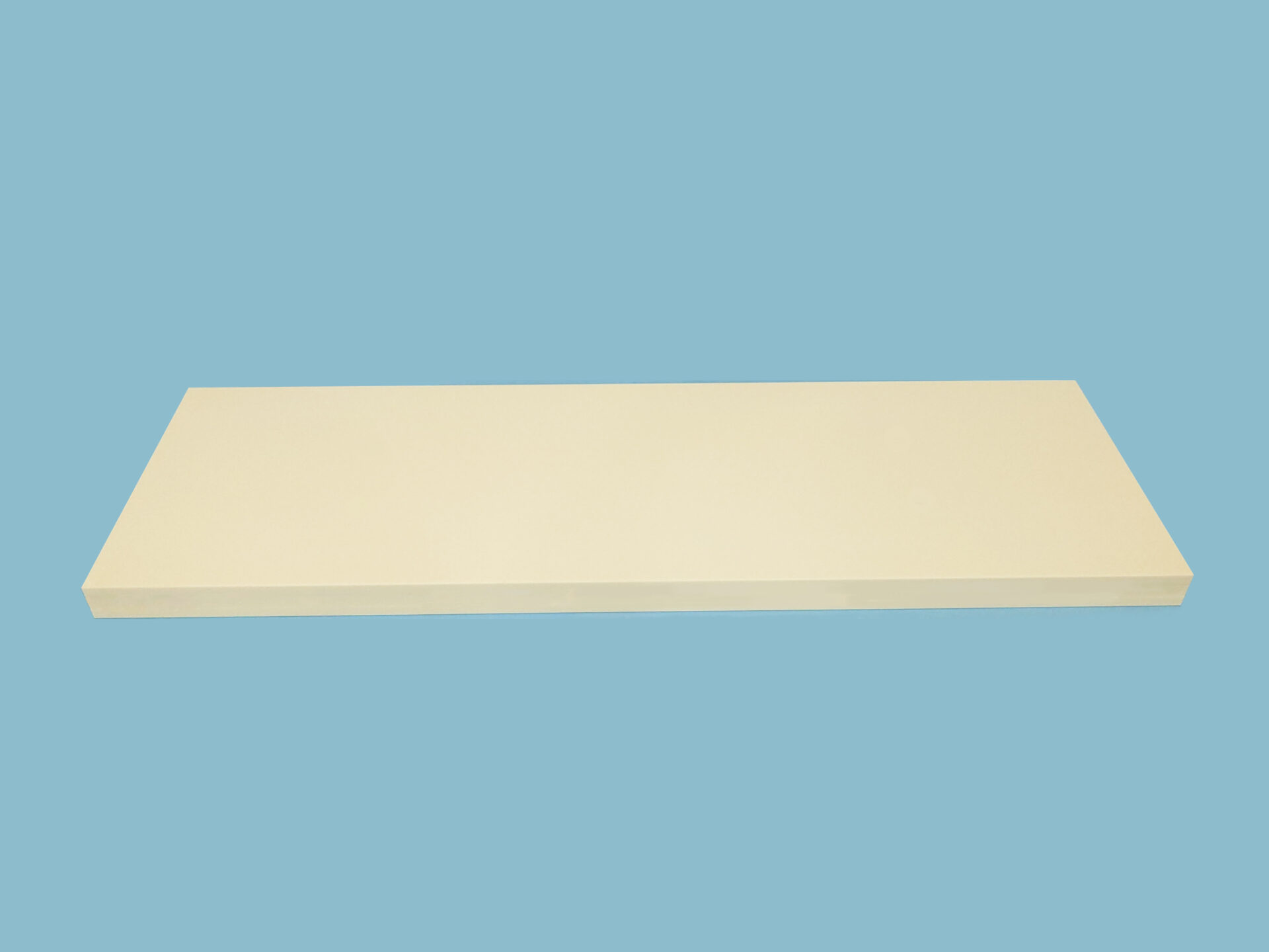
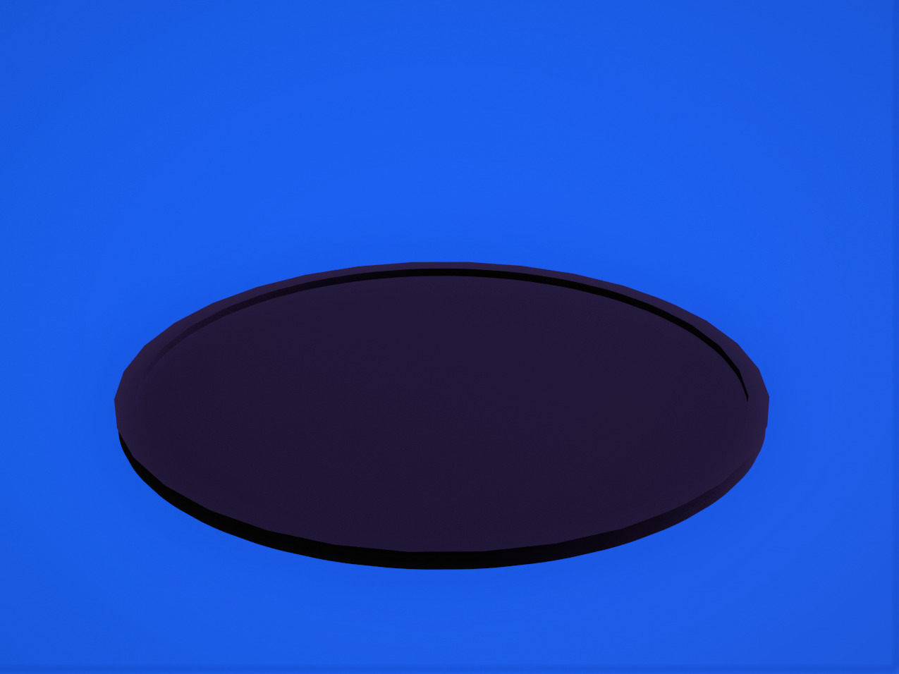
| Material | Porous Ceramics |
| Size | Body External diameter:Φ170 , Thickness 20 mm, Porous External diameter: Φ150 , Thickness 8 mm |
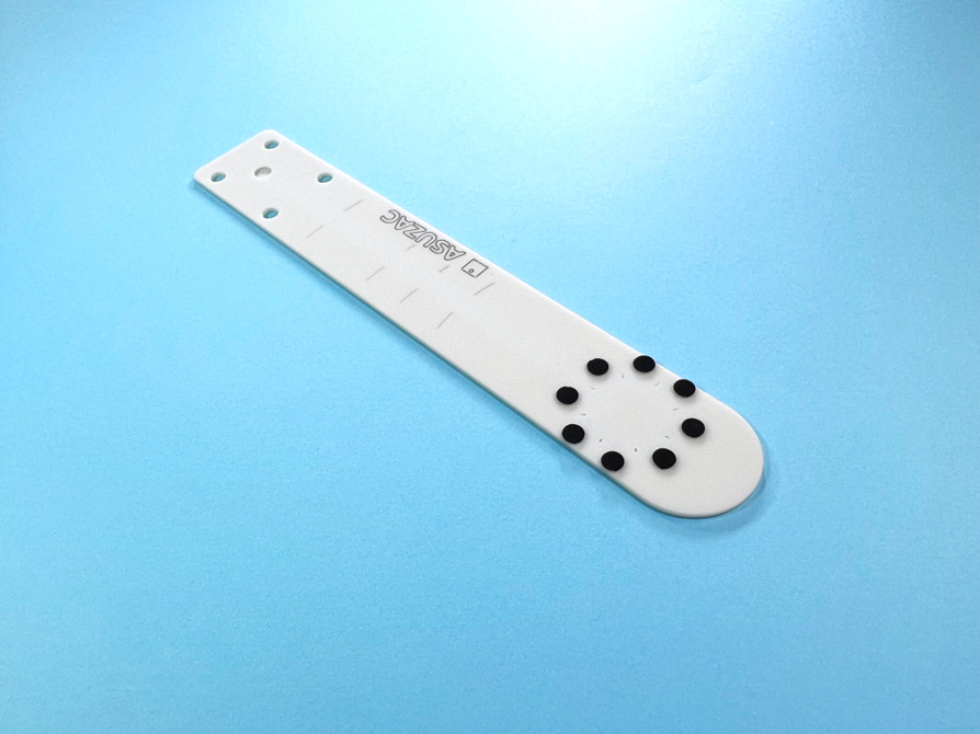
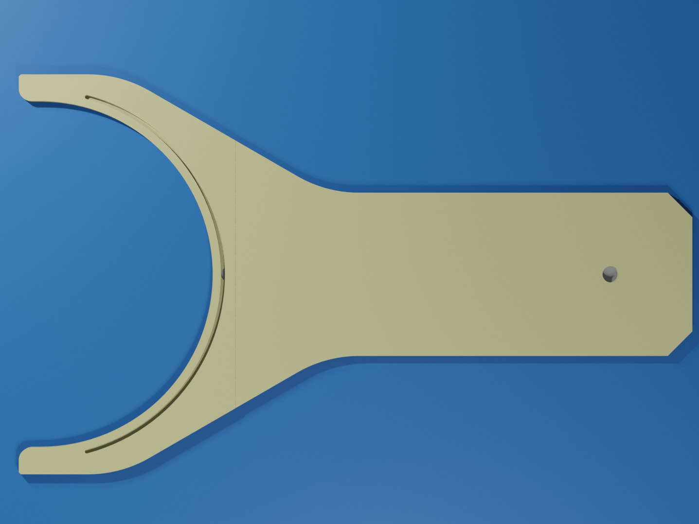
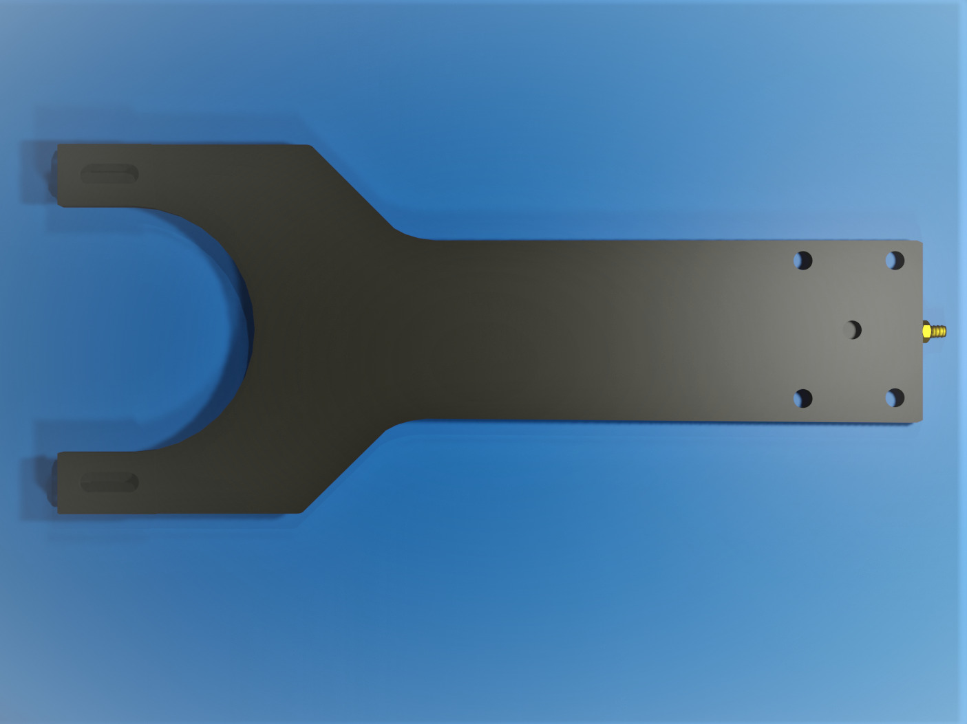
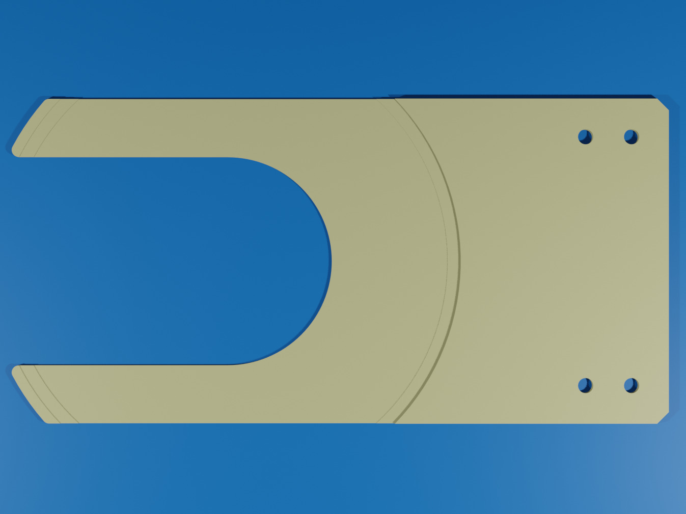
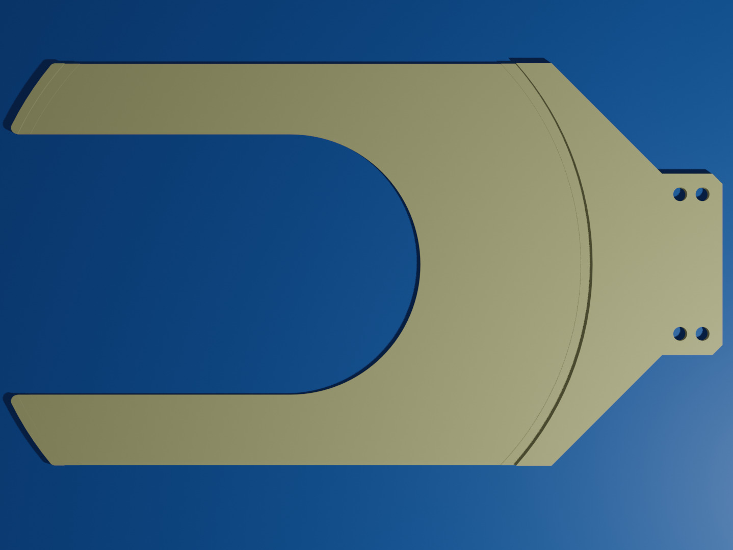
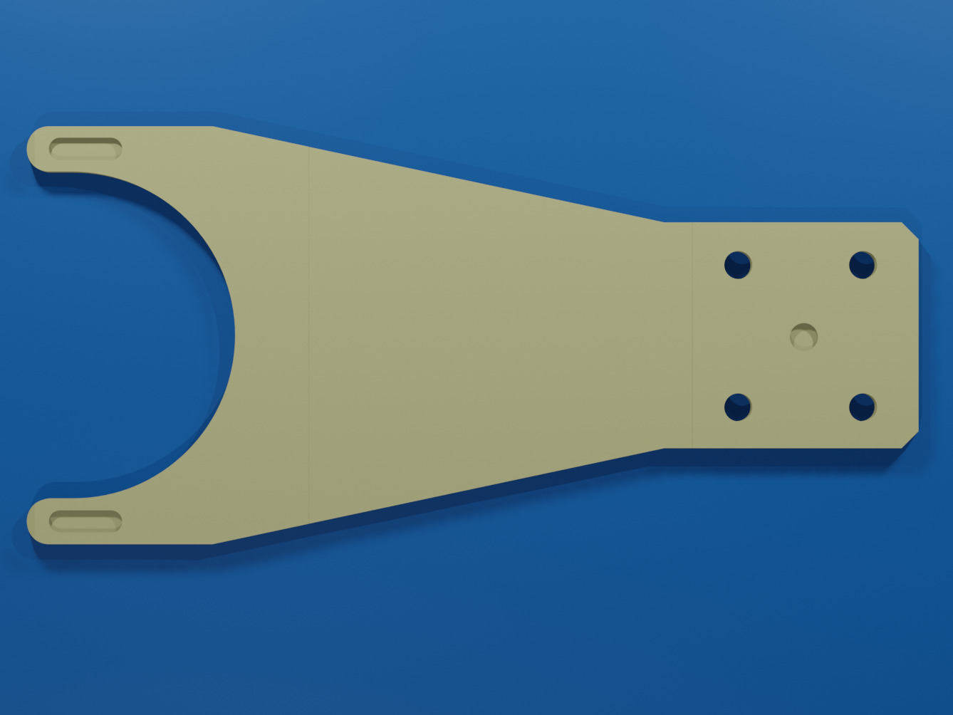
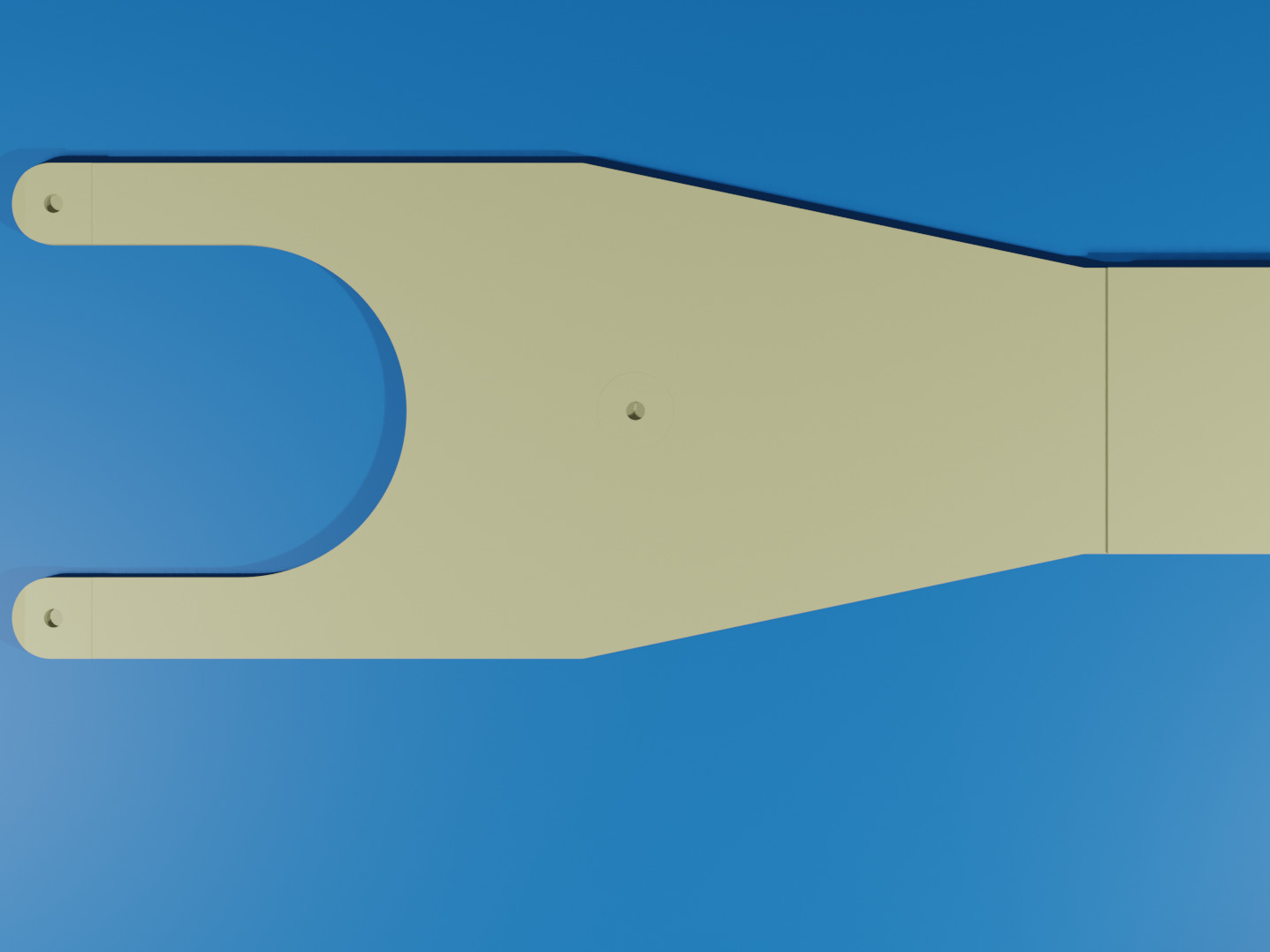
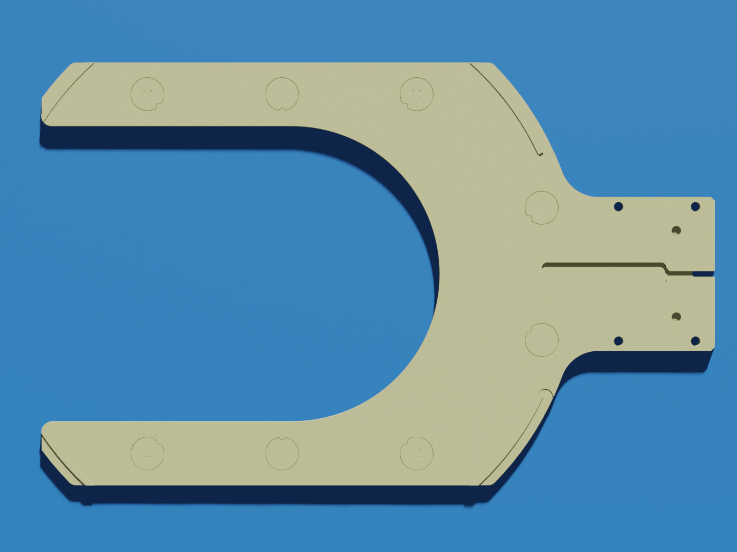
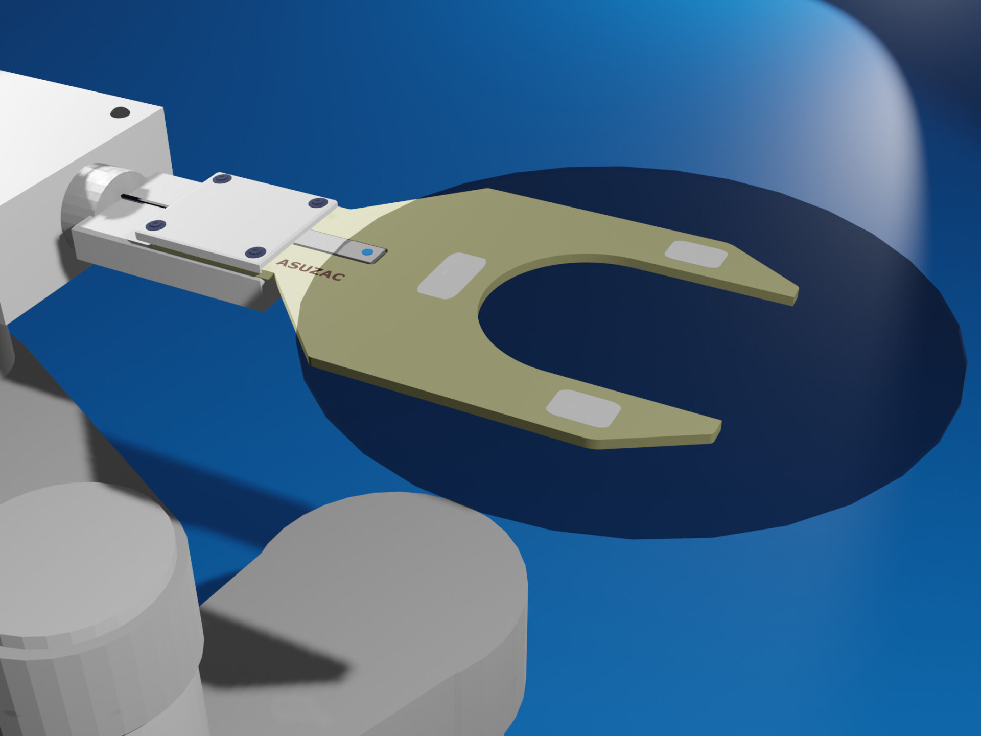
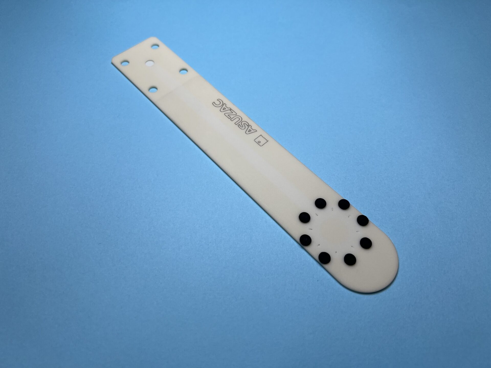
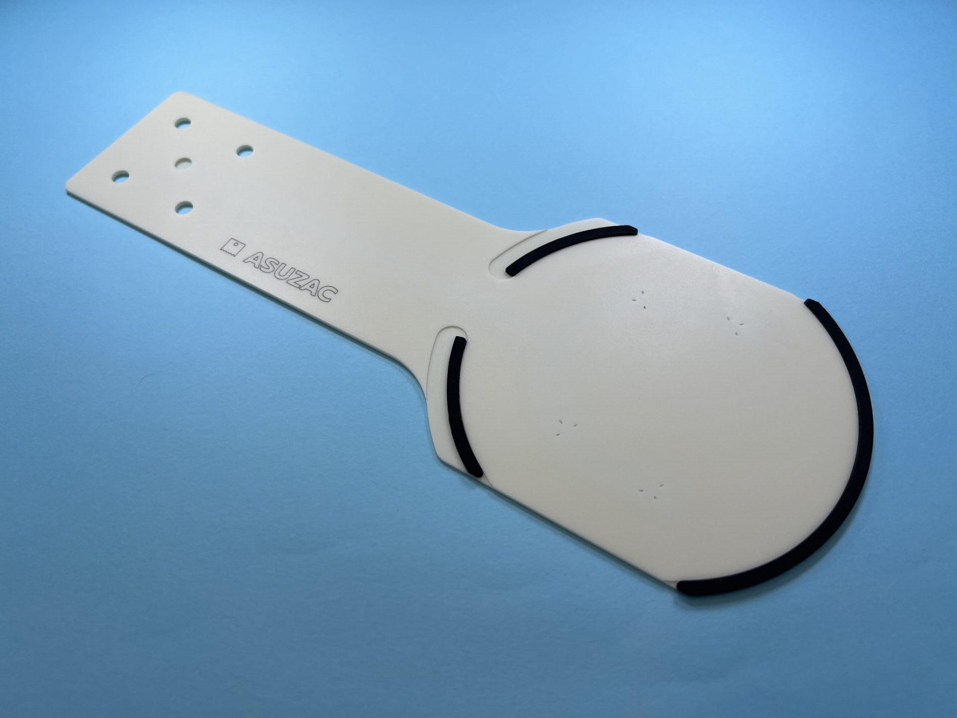
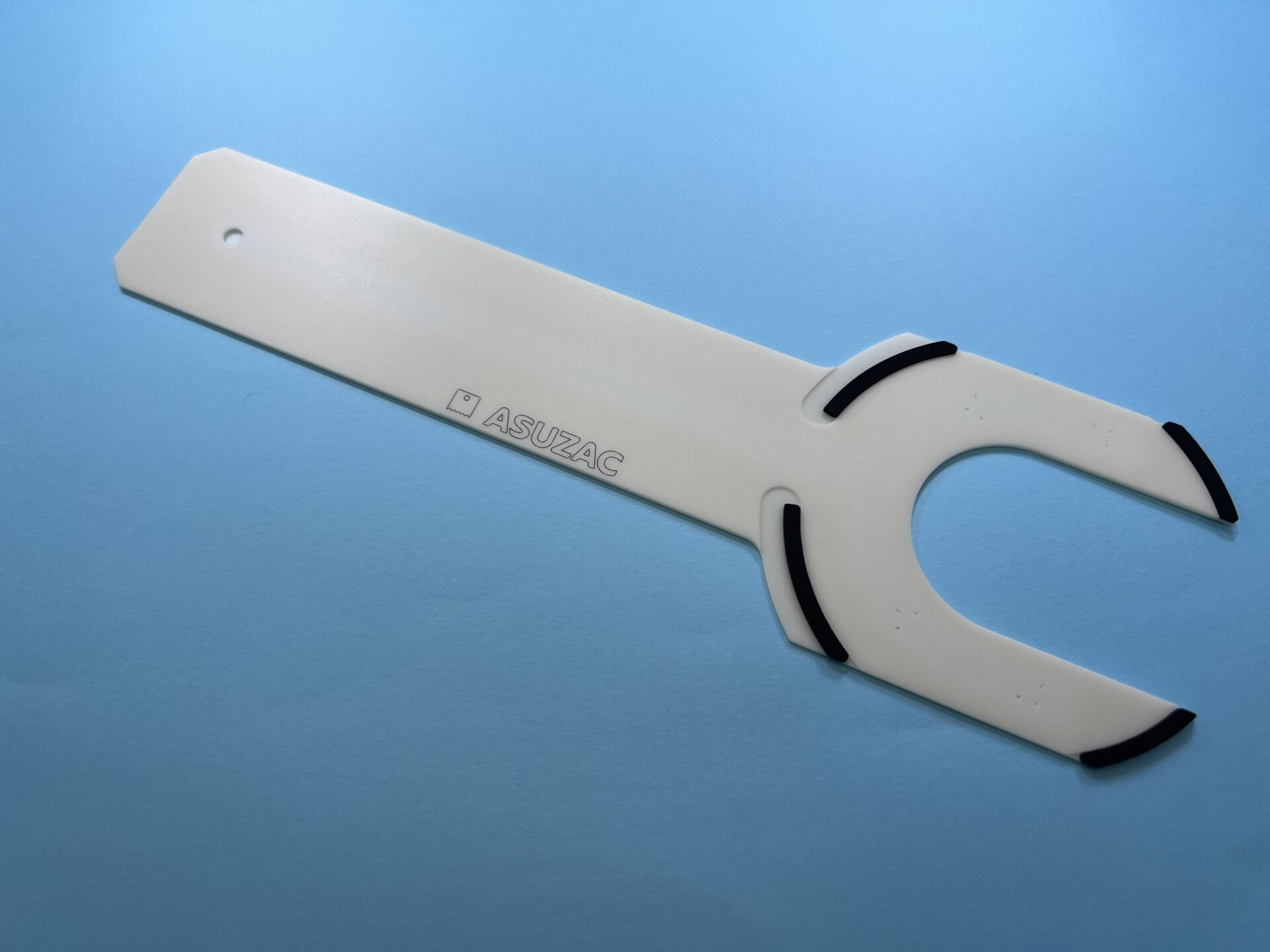
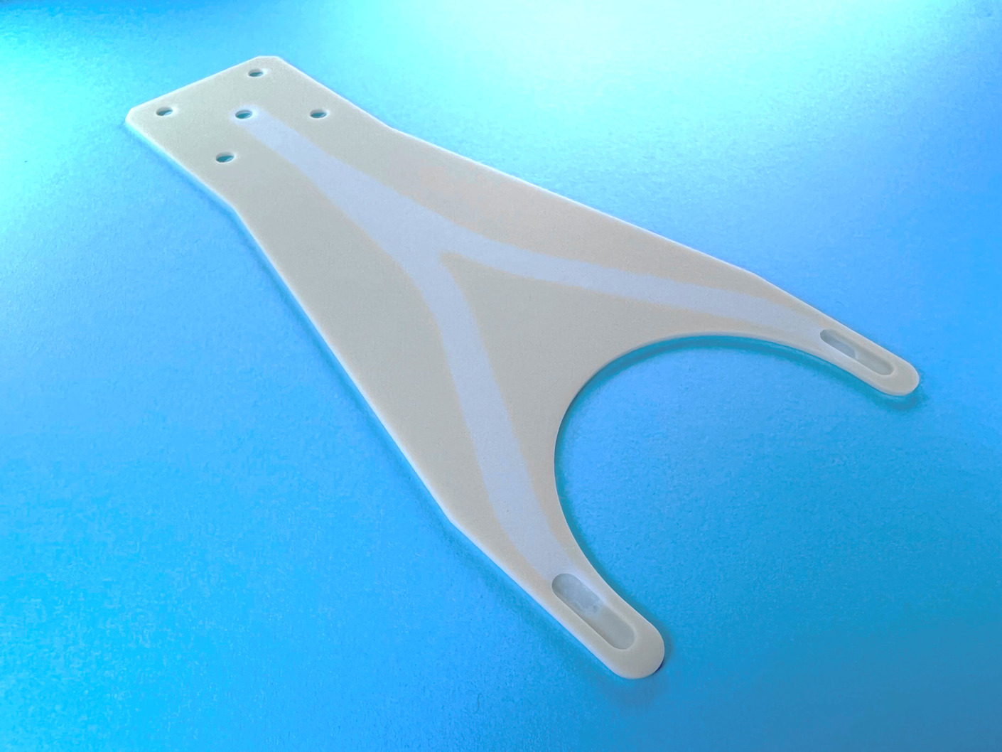
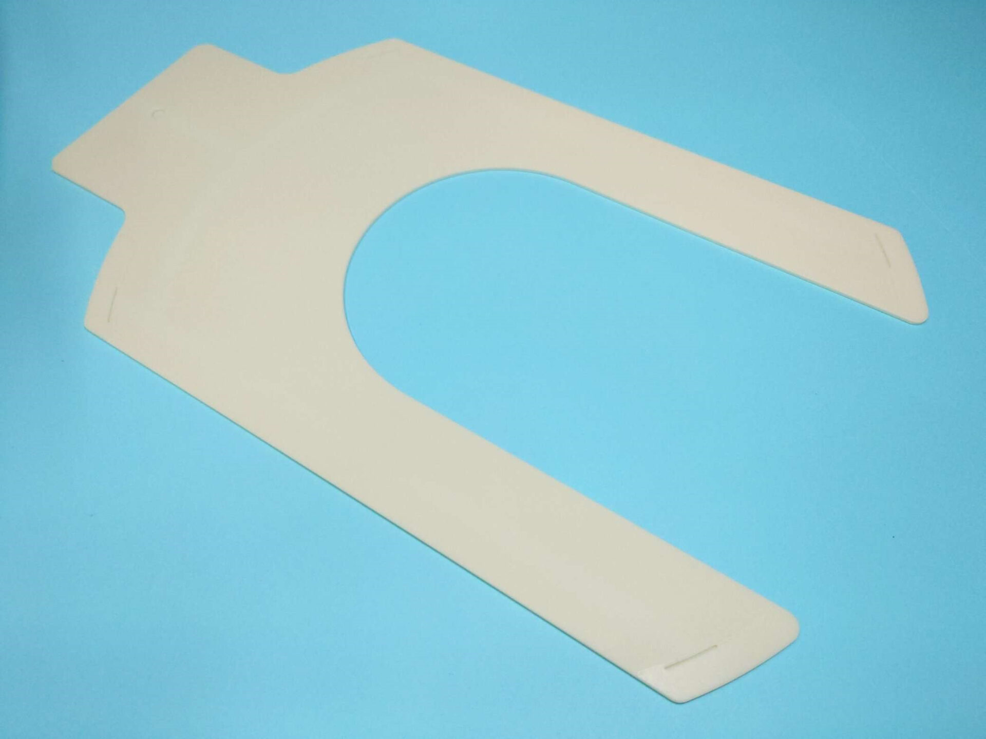
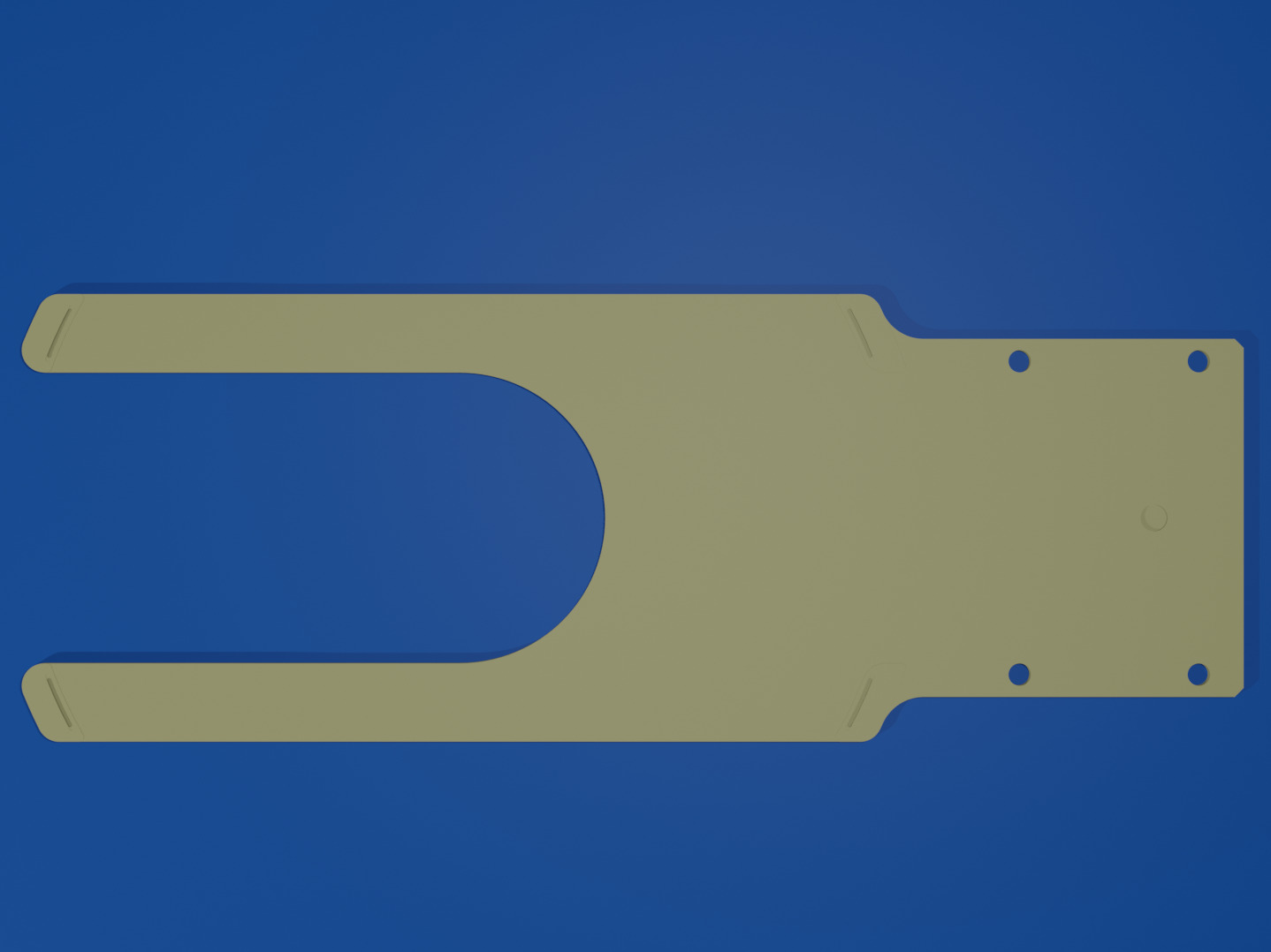
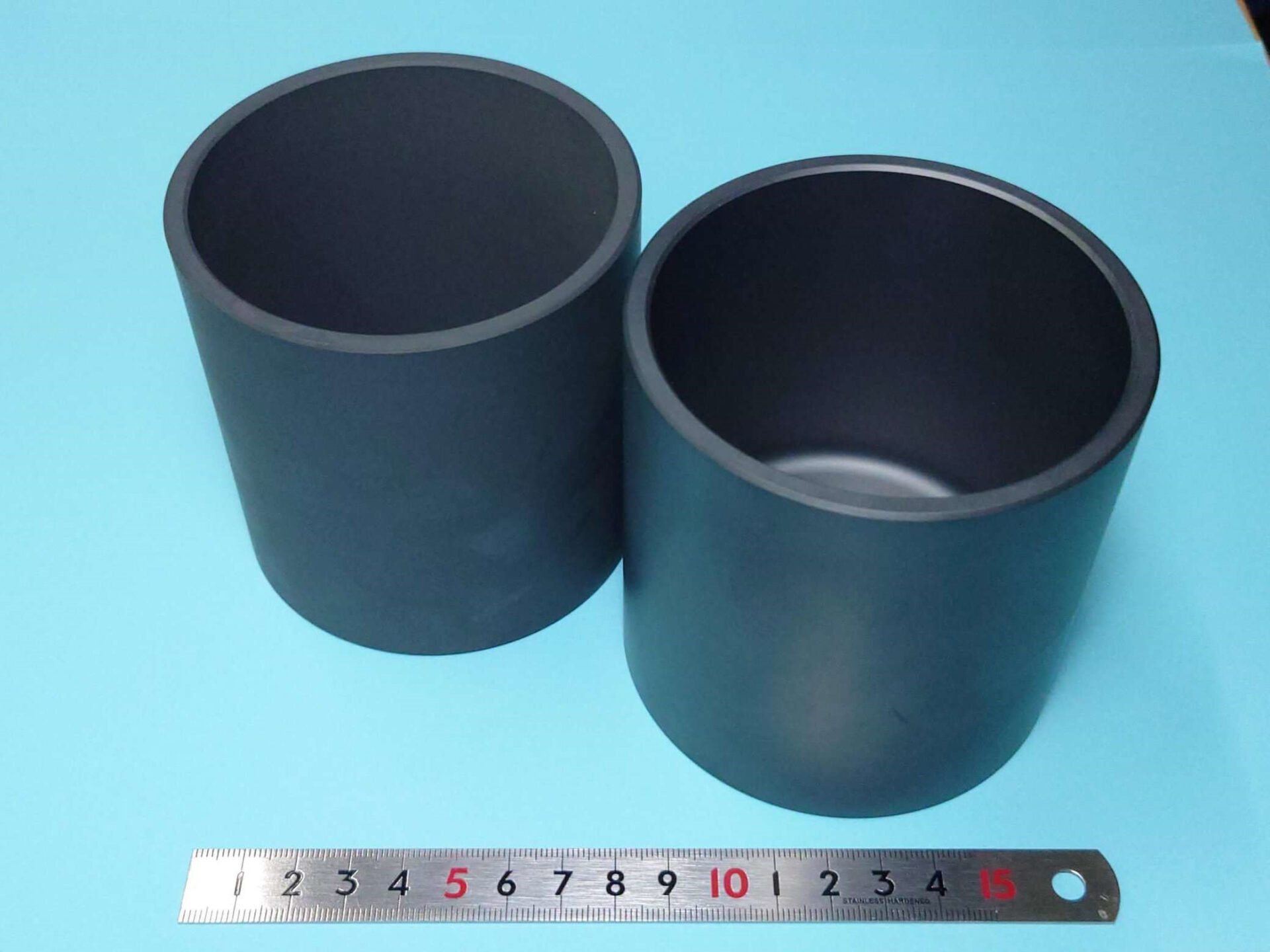
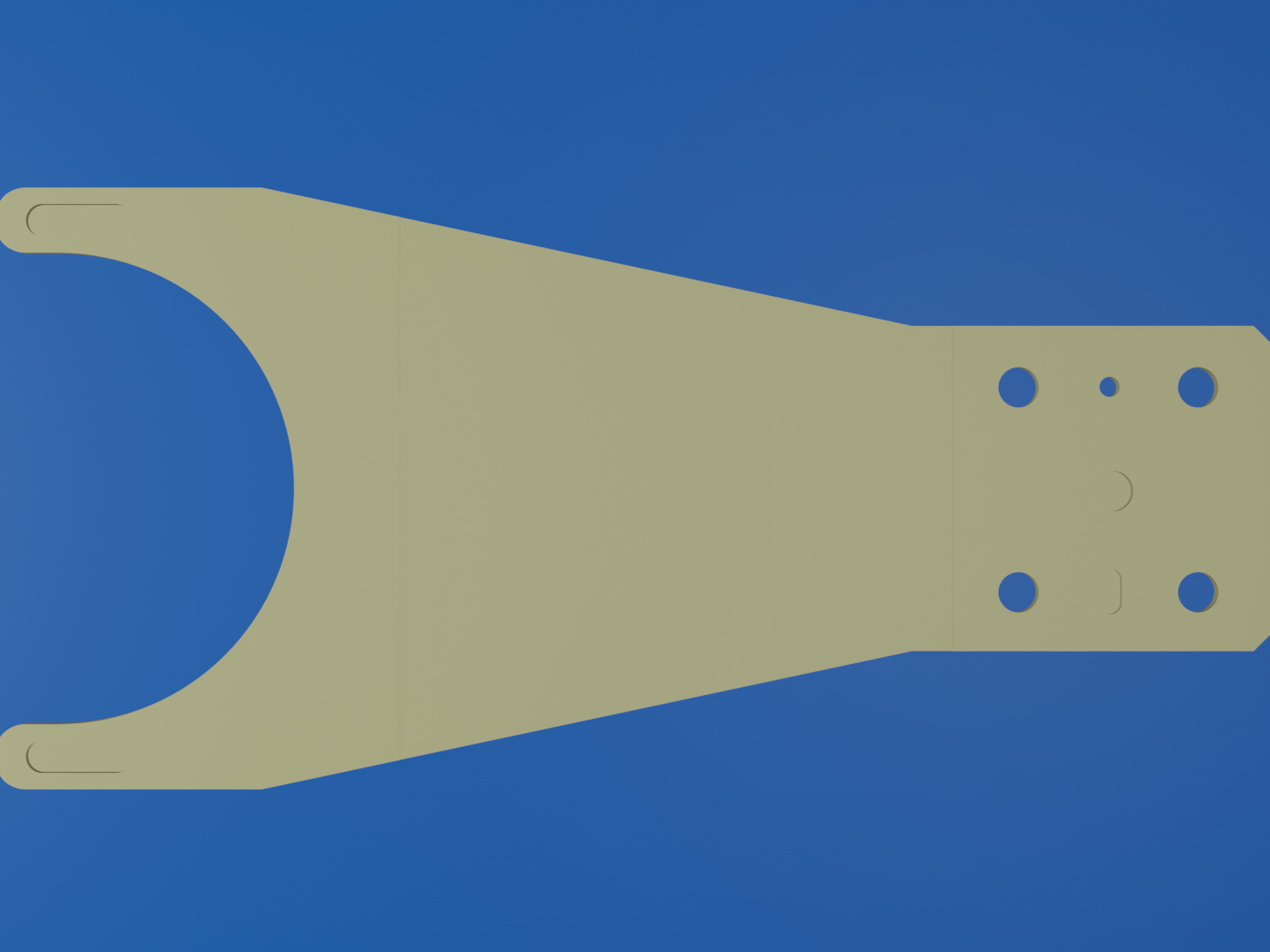
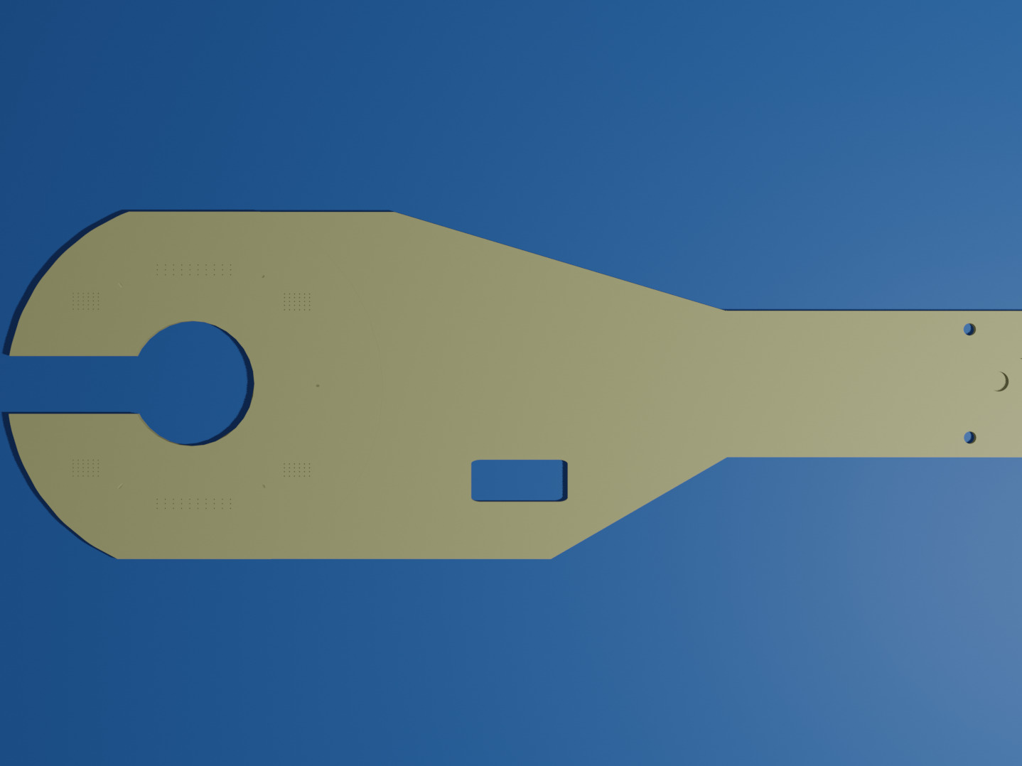
This is a porous chuck used to adsorb wafers, filters, and jigs.
We used our machining center to perform machining with JIS intermediate dimensional accuracy.
The amount of popping out of the porous part is 1mm.
Suction port (Rc1/8) is provided on the side of the main unit.
The porous and body are bonded with an epoxy-based adhesive.
Asuzac Corporation, which operates the Ceramics Design Lab, offers a full range of services from the preparation, granulation, and molding of porous ceramic raw materials to green processing (raw processing), firing, secondary processing, inspection, and cleaning.
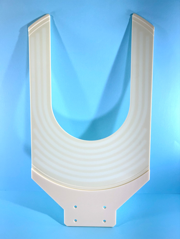
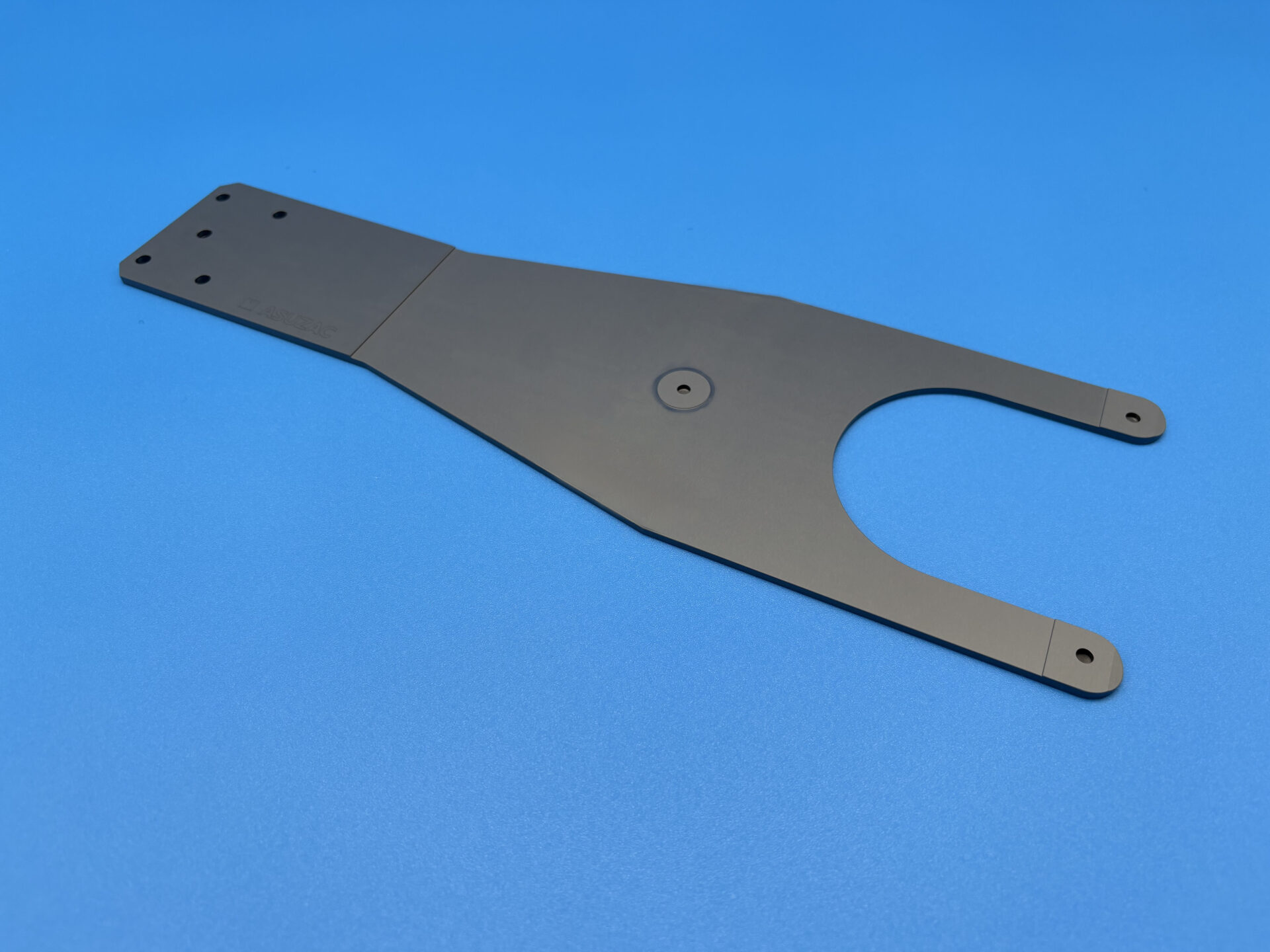
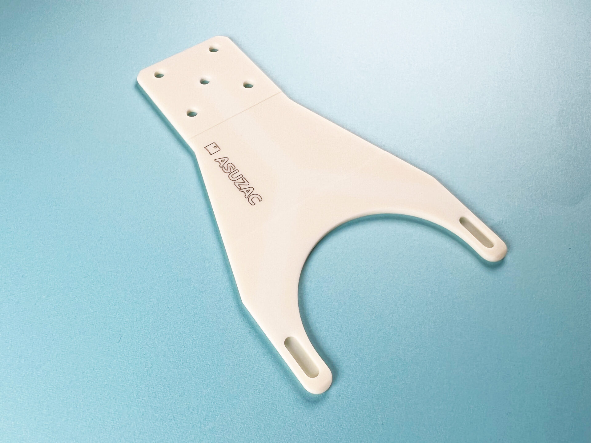
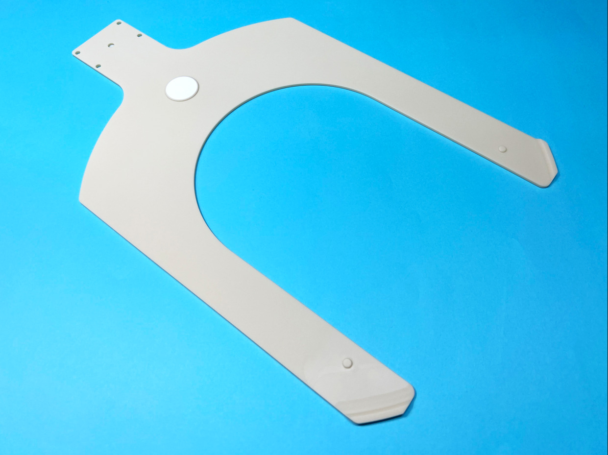
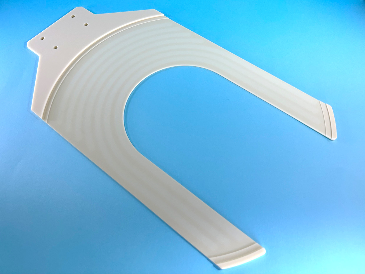
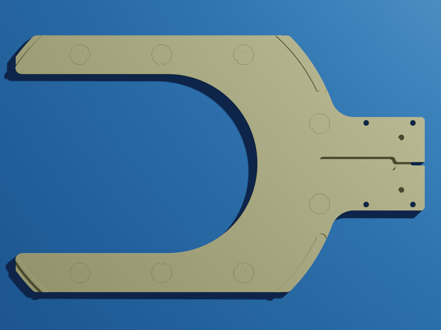
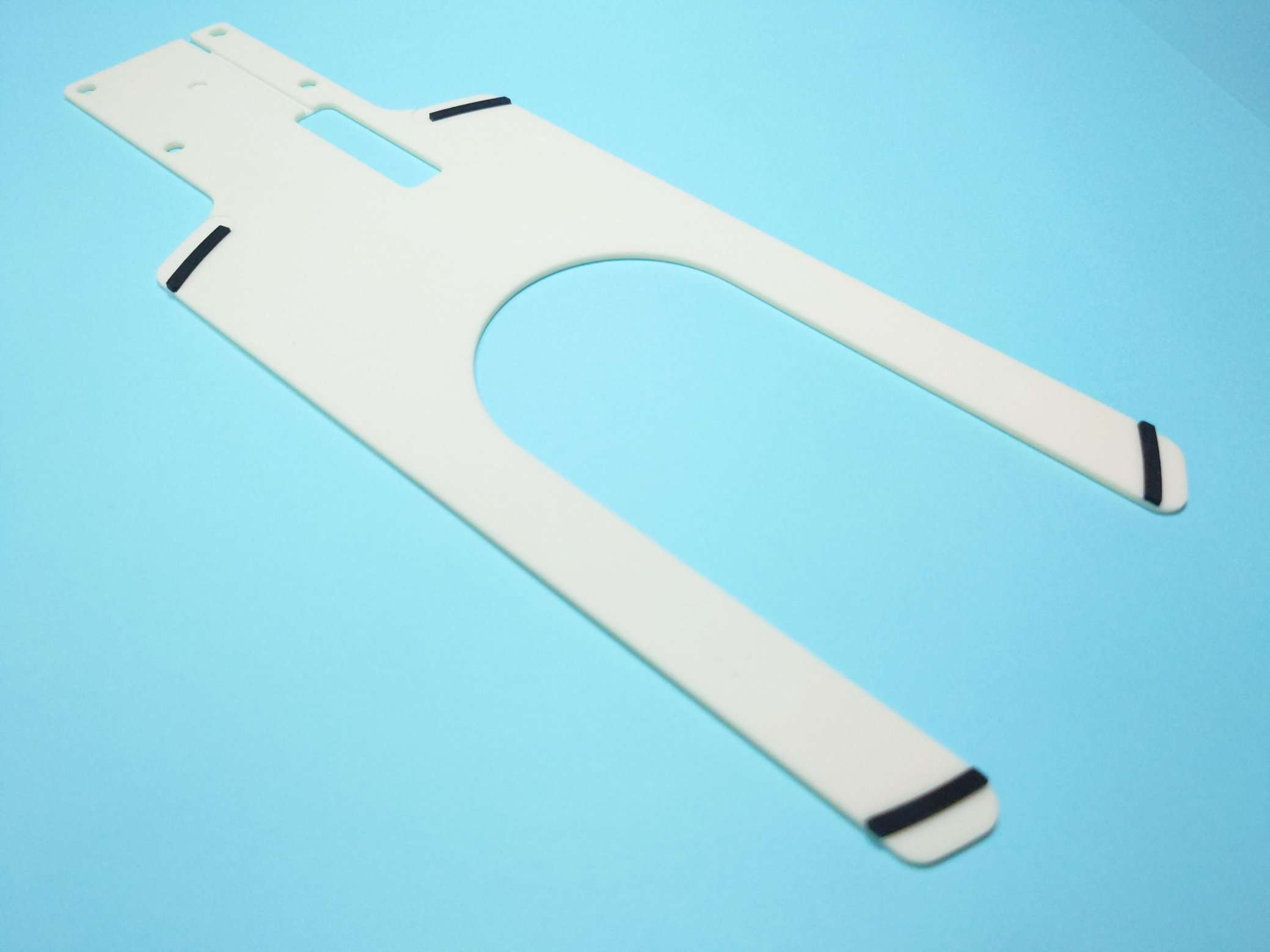
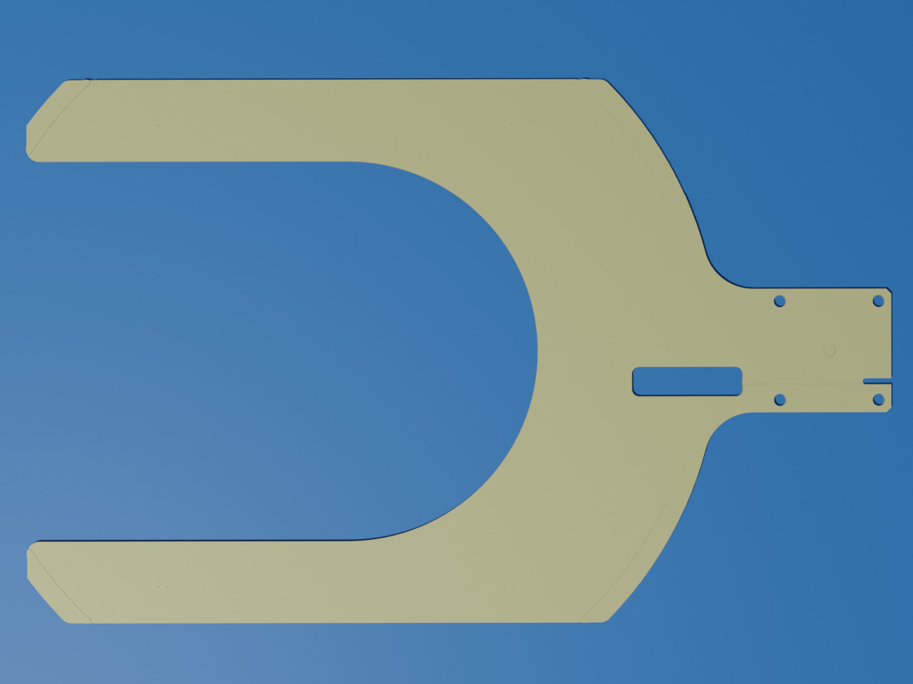
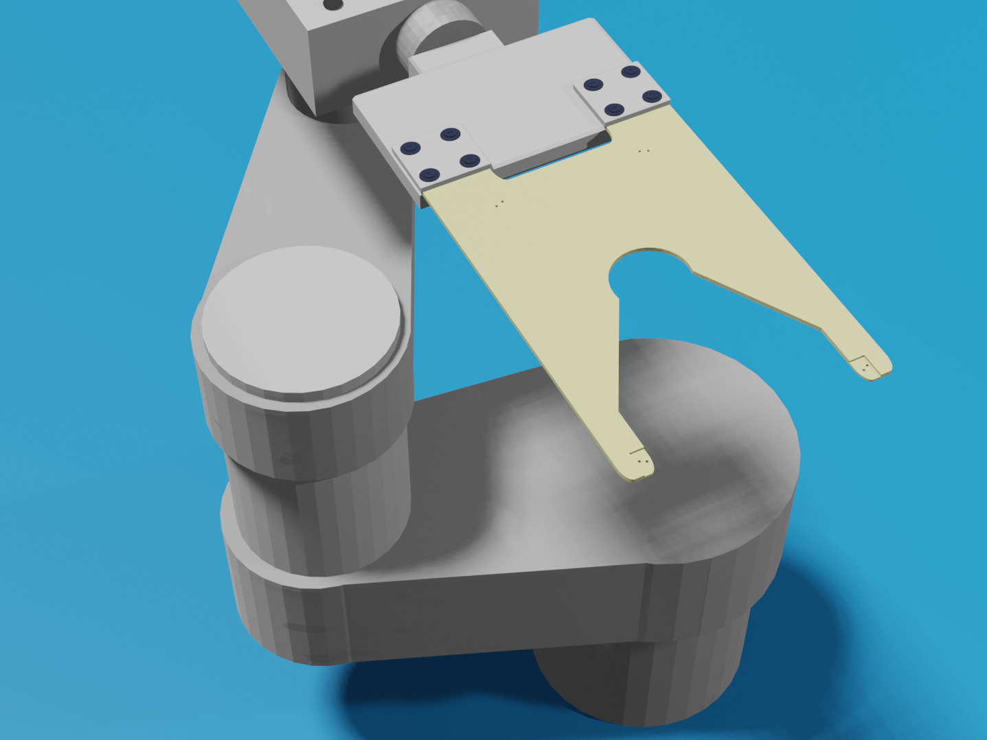
In addition to suction chucks such as this product, we have a large number of experience in manufacturing ceramics products such as wafer Transfer End Effector / Handling Arm, wafer trays, and sintering jigs.
For the design and manufacture of ceramics products for semiconductors and electronic components, leave it to Asuzac.
Integrated response from processing to development of ceramic materials !
Please feel free to contact us !
TEL +81-26-248-1626
Business hours: 9:00-17:00 (closed on Saturdays, Sundays and Holidays)
.jpg)
.jpg)
.jpg)
.jpg)
.jpg)
v1.jpg)
(本体アルミ、多孔質AZP60)v1.jpg)
.jpg)


(アスザックロゴ入り大きい).jpg)

.jpg)
_1.jpg)
v4.jpeg)
-v1.jpg)
外形120×80×厚み10mm-v1.jpg)

-1.jpg)
.jpg)
v1-1.jpg)
v1-1.jpg)