-
問題翹曲的晶圓
-
擬議效果晶圓翹曲對策
防止錯位
改進的功能 -
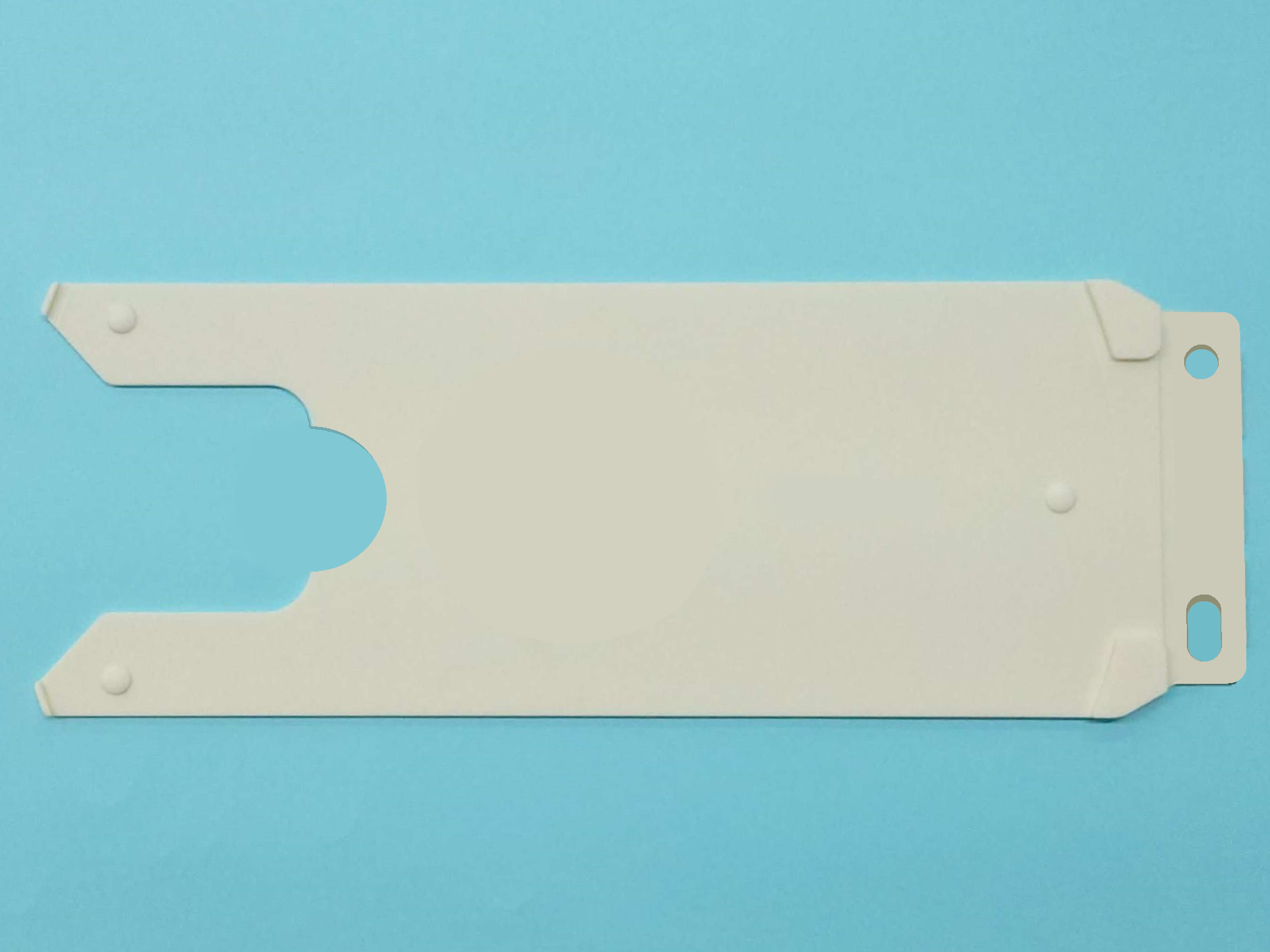
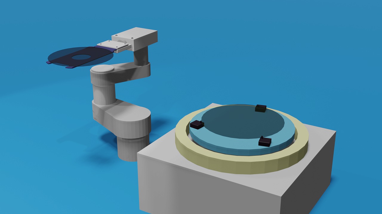
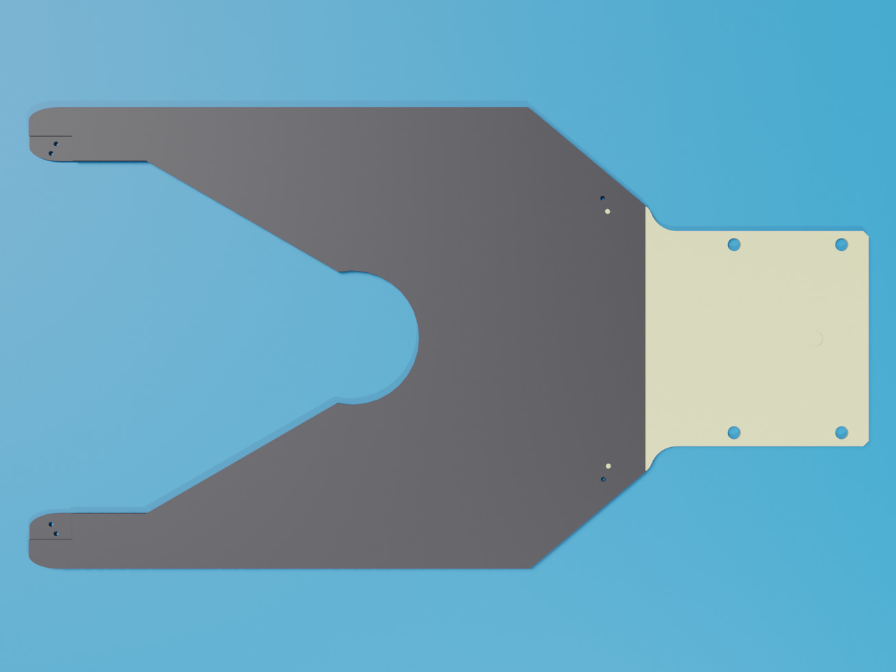
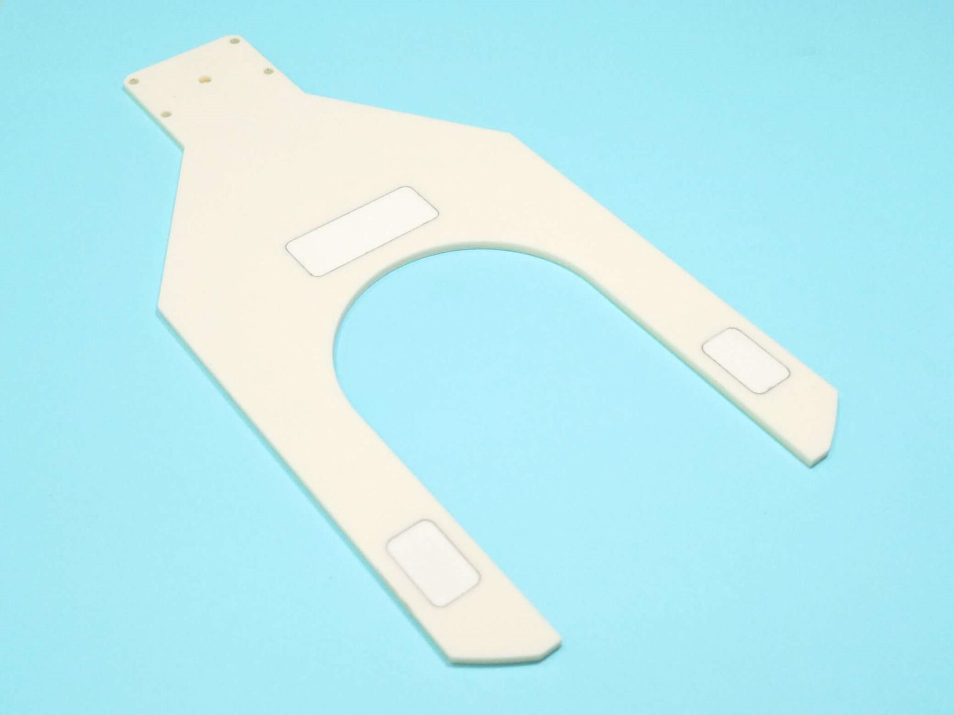
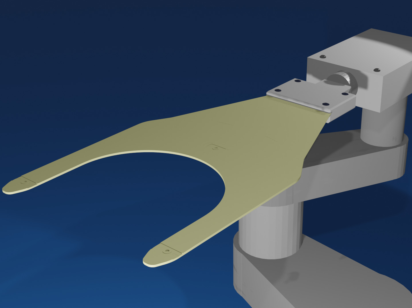
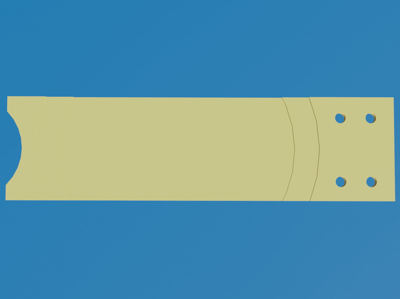
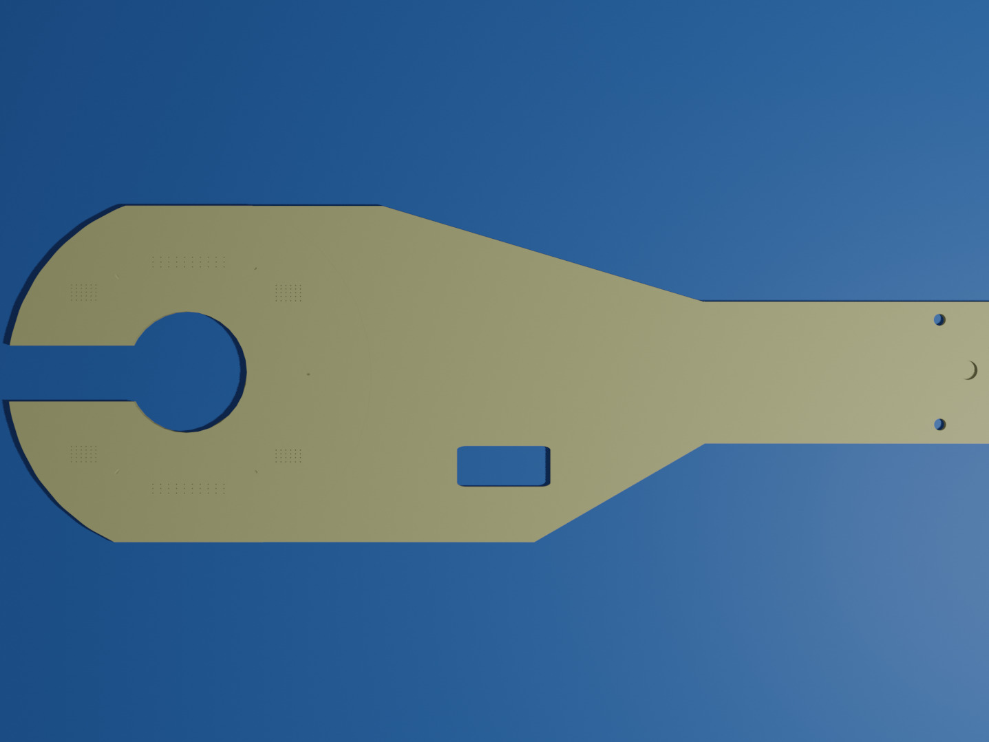
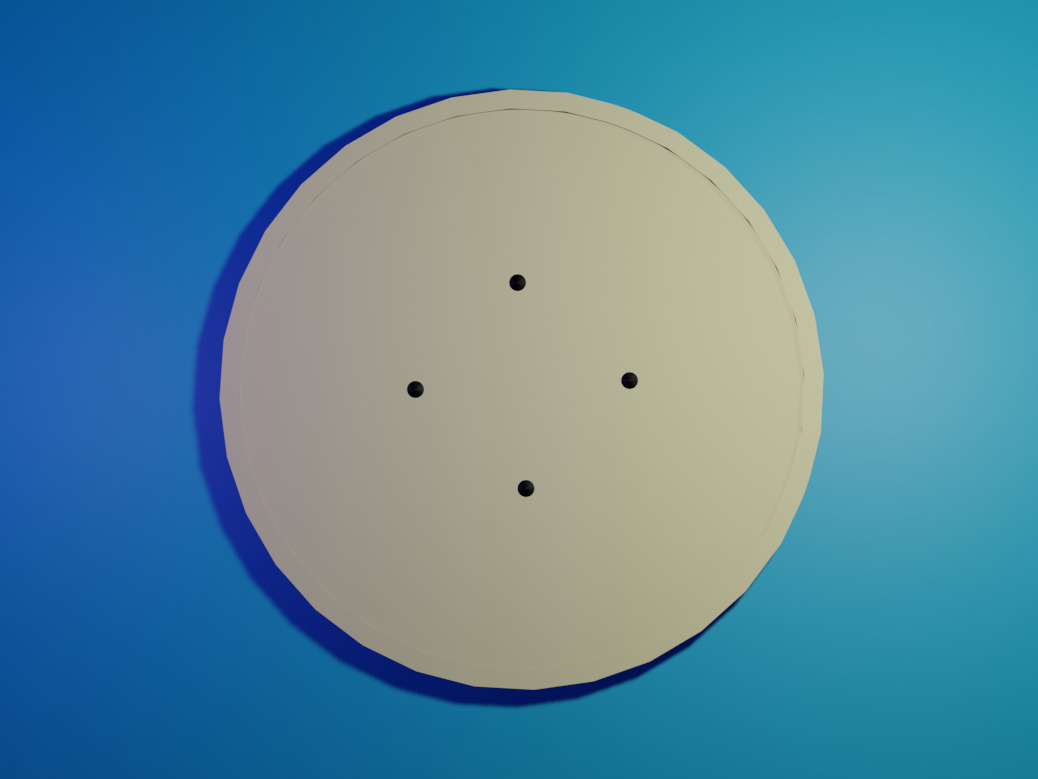
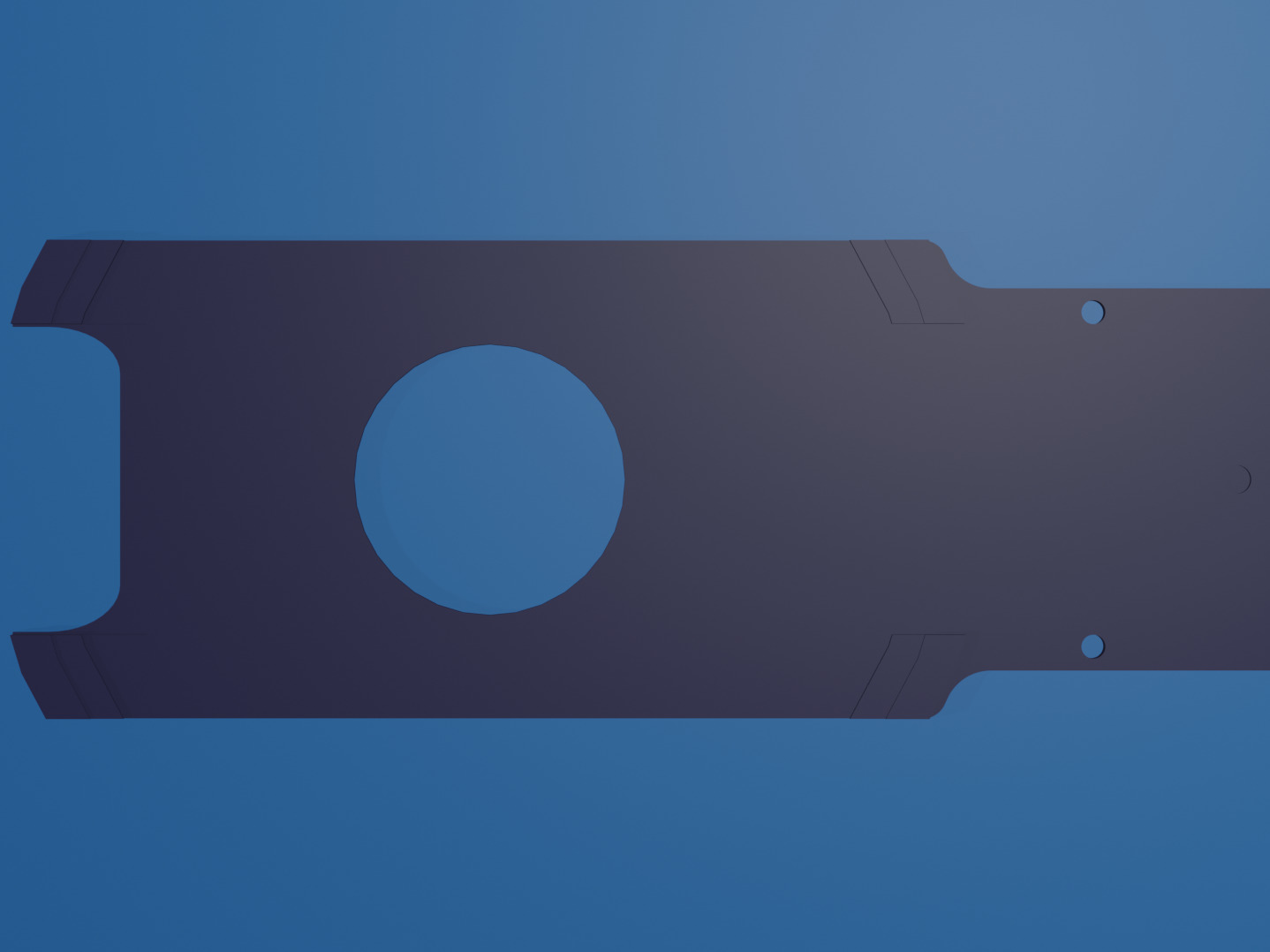
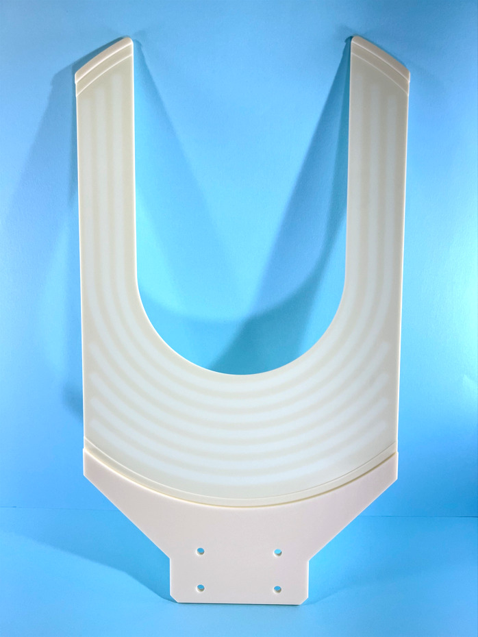
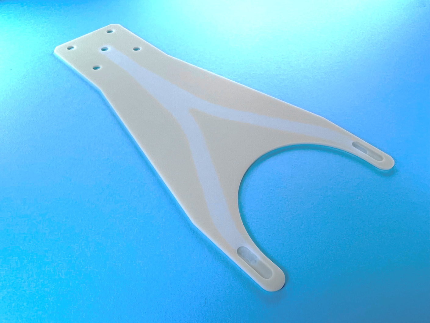
產品類別晶圓傳送手
客戶的疑慮和問題 / 之前
我們的建議及改善效果 / 完成後
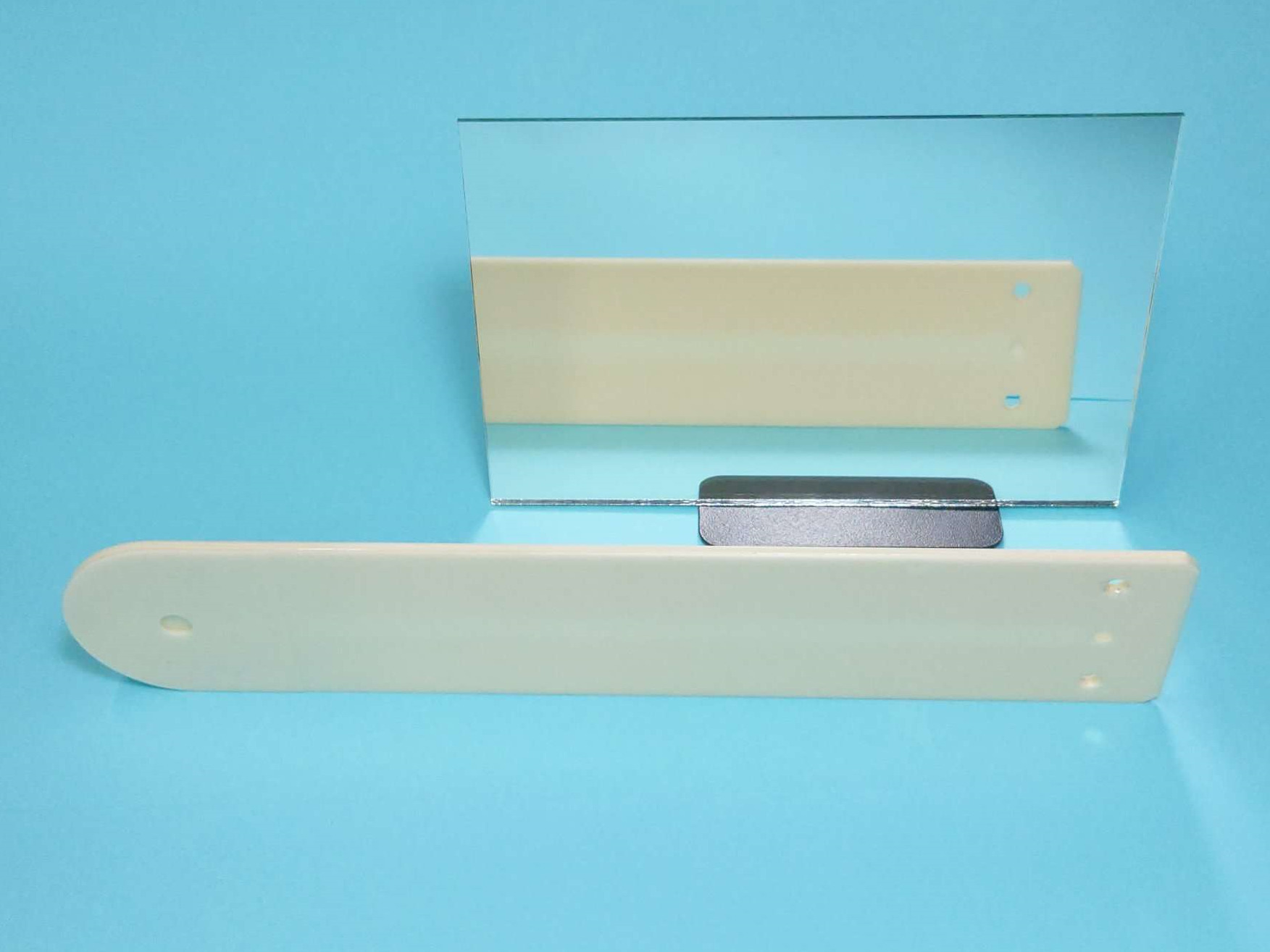
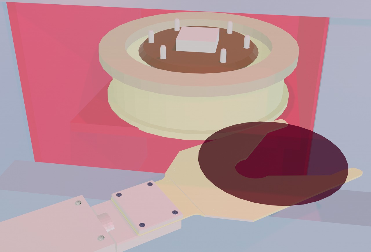
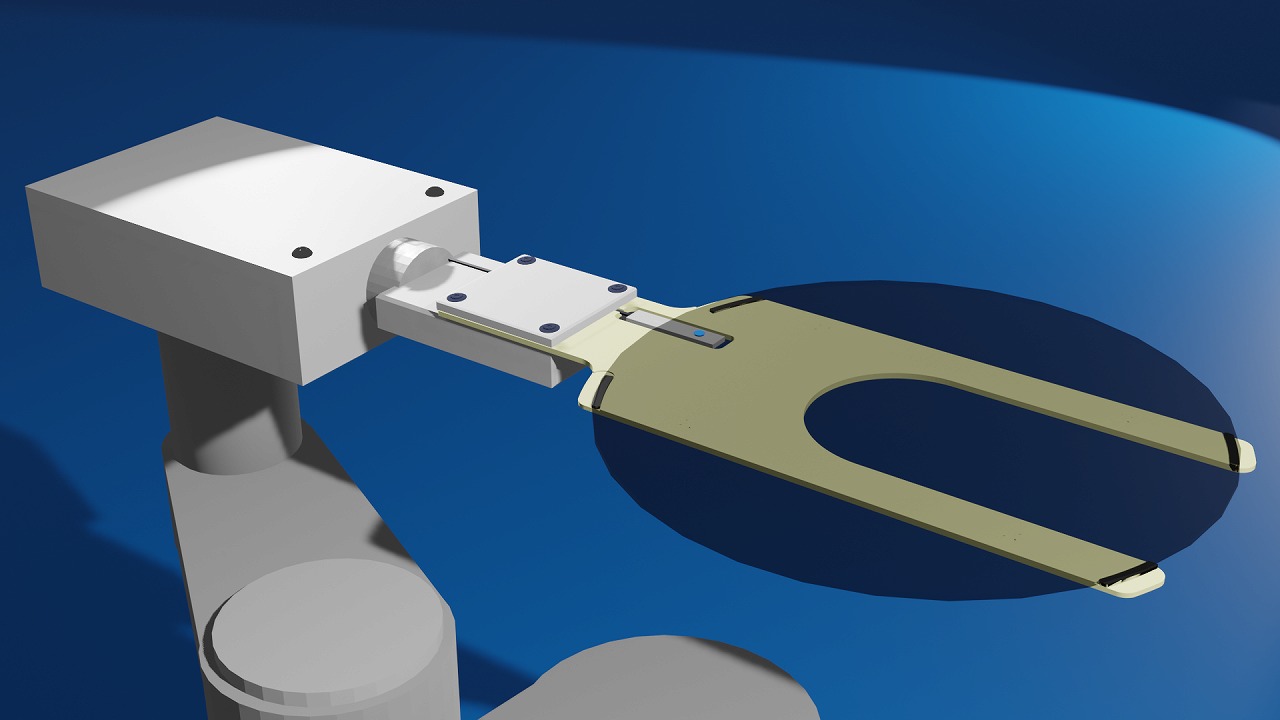
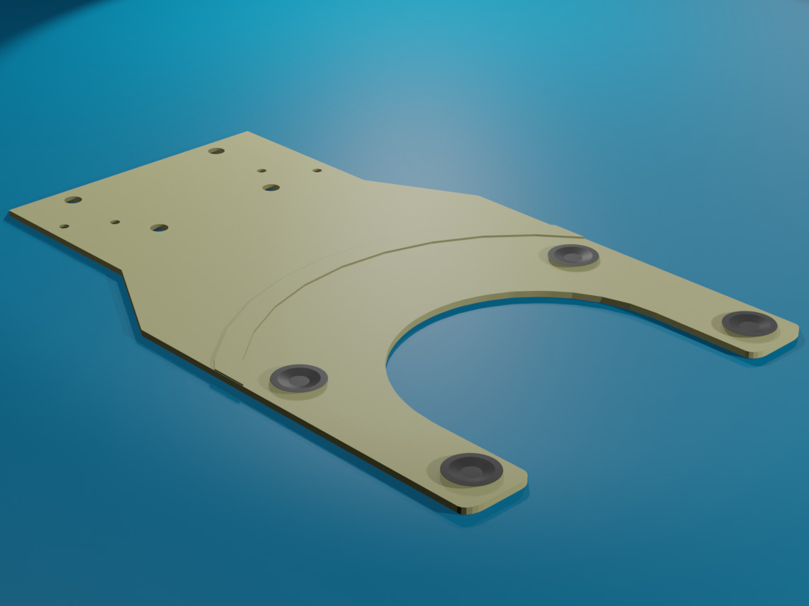
Therefore, in the Ceramic Design Laboratory, we proposed the Bernoulli End Effector LeviZac, which can stably hold thin wafers and suppress wafer misalignment.
This time, I-shaped LeviZac ® was designed and proposed according to the customer’s application.
As a result, we were able to reduce damage to thin wafers due to insufficient wafer retention or vacuum leakage, and wafer scratches, breakage, and defects due to wafer misalignment, thereby improving yield.
-1024x768.jpg)
-1024x768.jpg)
-1024x768.jpg)
-1024x768.jpg)
建議示例的要點/要點
The point of this case is that the thin wafer can be held stably and the misalignment of the wafer can be reduced.
When designing a transfer End Effector for thin wafers, it is necessary to design it considering reduction of suction shortage and vacuum leakage, etc.
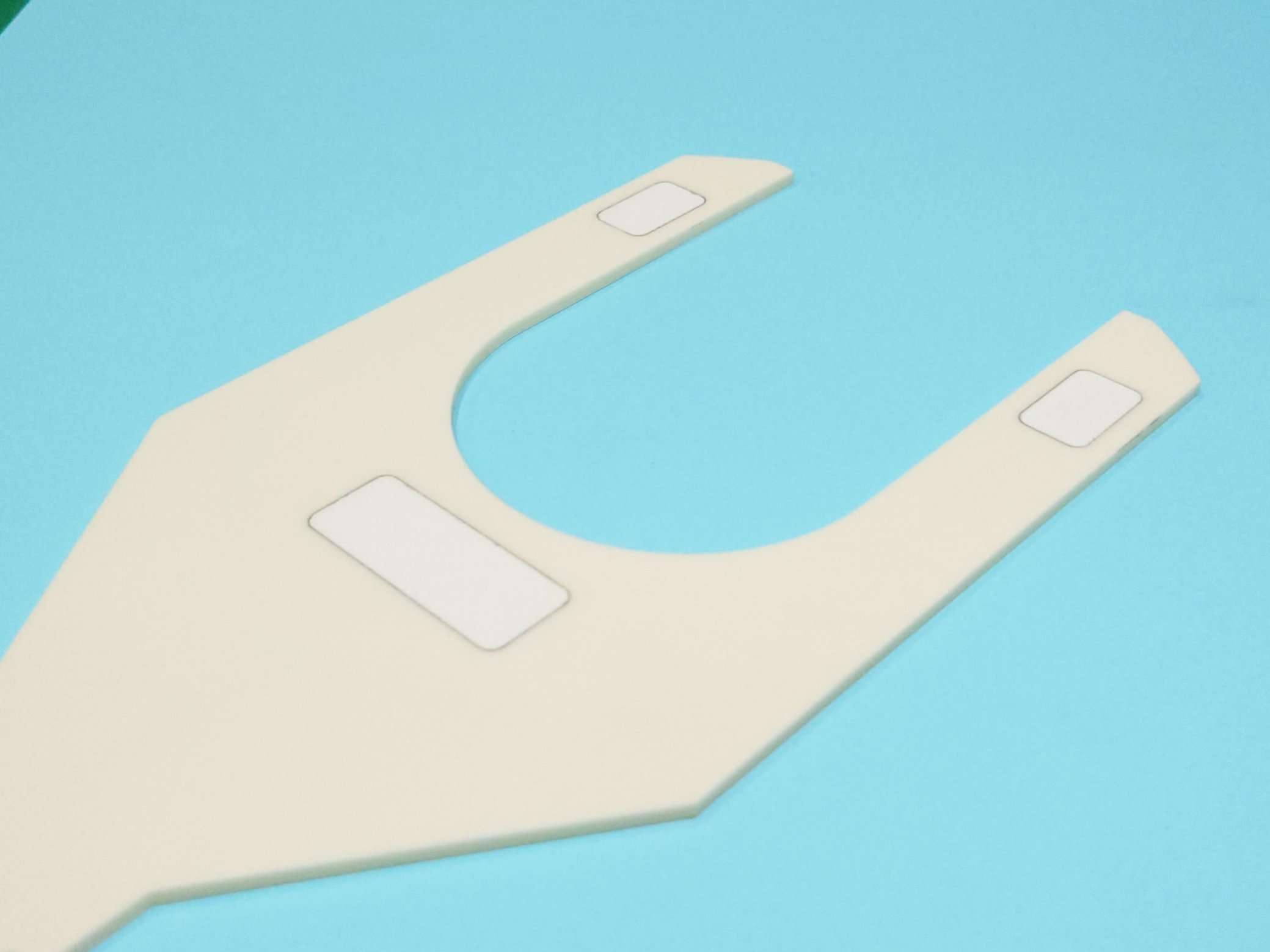
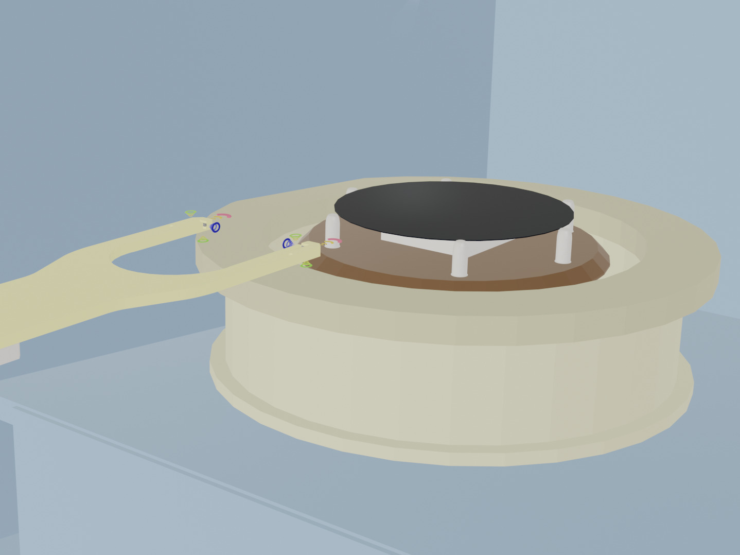
Since the wafer is held by eight guides, the thin wafer can be held stably.
In addition, since the misalignment of the wafer can be prevented, there is no effect on the surrounding workpiece due to air leakage.
The Fine Ceramics Division of ASUZAC Corporation, which operates the Ceramic Design Laboratory, handles everything from material development and preparation to design and manufacture, as well as surface treatment, inspection, and cleaning.
We can also offer our own coating-technology for adding functionality to ceramics materials, as well as the selection of materials such as ceramic materials with high heat resistance and conductivity, and high-purity alumina and SiC that are highly pure and prevent contamination.
Contact a Tsubaki representative if you are having trouble transporting thin wafers or misalignment of wafers.


.jpg)


.jpg)


A customer of a semiconductor/inspection equipment manufacturer asked us, “Can you suggest a End Effector that can transfer thin wafers and control wafer misalignment when transferring wafers from a wafer carrier during the wafer inspection process?”
They contacted us because we have lot of experience in manufacturing transfer End Effector !